


 Fresh PCB Concepts: IPC-6012 Class 3 and High-reliability PCB Manufacturing
 Elementary, Mr. Watson: The Display Revolution, Now With Fewer Tiny Keys
 Beyond Design: Skip-layer Routing—The Waveguide Structure That Makes 224G Possible


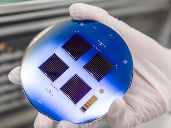
The efficiency of solar cells can be increased by thin-film contacts developed by researchers at KAUST.
A silicon solar cell that uses an electron-selective tantalum-nitride-metal contact for improved efficiency.
Improving the performance of solar cells requires scrutinizing every aspect of their design. First, this means improving the crystalline quality of the absorbing material to maximize the conversion of photons to negatively charged electrons and positively charged holes. Next, the device’s architecture must be optimized to ensure these charge carriers can move efficiently through the material. Finally, the electrical contacts that extract the carriers from the device and into an external circuit need to be perfected.
Xinbo Yang and his colleagues from the KAUST Solar Center and the KAUST Core Lab, together with coworkers from the Australian National University, focus on this third step by developing electron-selective tantalum-nitride thin-film contacts for silicon solar cells.
The interface between a silicon and a metal contact can create a high-resistance barrier that disrupts current flow. Additionally, the metal-induced electronic states at the surface of silicon enable the charge carrier to recombine, which reduces the conversion efficiency. Traditionally, high-cost processes, such as diffusion and chemical-vapor deposition of additional layers were adopted to reduce the contact resistance and carrier recombination.
The team led by Stefaan De Wolf (left) and Xinbo Yang (right) created a silicon solar cell that used an electron-selective tantalum-nitride-metal contact that improved the power conversion efficiency.
Yang and the team combat these problems by placing tantalum nitride on silicon using a method known as atomic-layer deposition: they do this by exposing the surface to a gas, causing a high-quality thin film to build up one atom at a time.
“Electron-selective tantalum-nitride contacts can simultaneously reduce the charge carrier recombination and contact resistance,” explains Yang. “This can simplify the complexity of fabricating the device and lower the production cost.”
By experimentally investigating the electrical properties of the tantalum nitride–silicon interface, the researchers showed that the tantalum nitride interlayer was able to reduce the contact resistance to the flow of electrons from silicon and metal contacts made of silver or aluminum. But, it simultaneously blocked the flow of holes, reducing the carrier recombination
The team created a silicon solar cell that used an electron-selective tantalum-nitride-metal contact. They showed that this improved the power conversion efficiency—the ratio between electrical power out to optical power in—by more than 20 percent over a control device built without the tantalum nitride. They also found that it simplified the device fabrication sequence, and cost, by eliminating doping and contact opening processes.
“We are also investigating the potential application of tantalum nitride electron transport layers for organic and perovskite solar cells,” explain KAUST scientist and principal investigator, Stefaan De Wolf.


