-

- News
- Books
Featured Books
- design007 Magazine
Latest Issues
Current Issue
Signal Integrity
If you don’t have signal integrity problems now, you will eventually. This month, our expert contributors share a variety of SI techniques that can help designers avoid ground bounce, crosstalk, parasitic issues, and much more.

Proper Floor Planning
Floor planning decisions can make or break performance, manufacturability, and timelines. This month’s contributors weigh in with their best practices for proper floor planning and specific strategies to get it right.

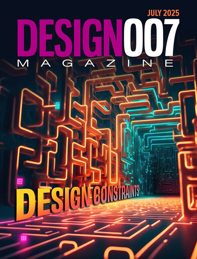
Showing Some Constraint
A strong design constraint strategy carefully balances a wide range of electrical and manufacturing trade-offs. This month, we explore the key requirements, common challenges, and best practices behind building an effective constraint strategy.
- Articles
- Columns
- Links
- Media kit
||| MENU - design007 Magazine
Imec Coordinates EU Chips Design Platform
May 9, 2025 | ImecEstimated reading time: 1 minute
A consortium of 12 European partners, coordinated by imec, has been selected in the framework of the European Chips Act to develop the EU Chips Design Platform. Funded by Chips JU, the platform will facilitate access to advanced semiconductor design infrastructure, training, and capital for fabless semiconductor startups, small and medium enterprises and research organizations. By providing the necessary resources, the initiative aims to democratize and foster semiconductor innovation across Europe, specifically for chip design.
The semiconductor industry is the backbone of modern technology, powering everything from smartphones to advanced medical devices. With the EU Chips Act, Europe is dedicated to increasing its global semiconductor market share. Next to the launch of European pilot lines that aim to develop key technologies for semiconductor innovation, the EU Chips Act has proposed the EU Chips Design Platform as a vehicle to support the growth of fabless chip companies in Europe.
The EU Chips Design Platform will enable fabless companies to access the resources they need quickly and efficiently via a cloud-based virtual environment, offering chip design resources, training, and capital. Coordinated by imec, twelve key European research players in the semiconductor ecosystem have joined forces in a consortium to create this design platform.
The platform aims to onboard the first startups and small and medium enterprises by early 2026, providing them with low-barrier access to European design capabilities, including route-to-chip fabrication, packaging, and testing. It will offer customized support to access commercial electronic design automation (EDA) tools, intellectual property (IP) libraries, EU Chips Act pilot line technologies, and access to design IP repositories, including open-source options. Additionally, the platform will feature a startup support program with incubation, acceleration, and mentoring activities next to financial assistance to help early-stage companies turn their innovative ideas into reality.
“The EU Chips Design Platform will provide crucial resources for startups and SMEs to accelerate their design journey and bring their business ideas to market faster. By reducing the barriers to access of design expertise, including EDA tools and IP, and drastically lowering chip design and fabrication costs and time-to-market, we will spark the growth of the European chip design industry,” stated Romano Hoofman, imec project coordinator.
Testimonial
"The I-Connect007 team is outstanding—kind, responsive, and a true marketing partner. Their design team created fresh, eye-catching ads, and their editorial support polished our content to let our brand shine. Thank you all! "
Sweeney Ng - CEE PCBSuggested Items
Deca, Silicon Storage Technology Announce Strategic Collaboration to Enable NVM Chiplet Solutions
09/11/2025 | Microchip Technology Inc.As traditional monolithic chip designs grow in complexity and increase in cost, the interest and adoption of chiplet technology in the semiconductor industry also increases.
I-Connect007 Launches New Podcast Series on Ultra High Density Interconnect (UHDI)
09/10/2025 | I-Connect007I-Connect007 is excited to announce the debut of its latest podcast series, which shines a spotlight on one of the most important emerging innovations in electronics manufacturing: Ultra-High-Density Interconnect (UHDI). The series kicks off with Episode One, “Ultra HDI: What does it mean to people? Why would they want it?” Host Nolan Johnson is joined by guest expert John Johnson, Director of Quality and Advanced Technology at American Standard Circuits (ASC).
Global Citizenship: Together for a Perfect PCB Solution
09/10/2025 | Tom Yang -- Column: Global CitizenshipIf there’s one thing we’ve learned in the past few decades of electronics evolution, it’s that no region has a monopoly on excellence. Whether it’s materials science breakthroughs in Europe, manufacturing efficiencies in China, or design innovations in Silicon Valley, the PCB industry thrives on collaboration.
The Shaughnessy Report: Winning the Signal Integrity Battle
09/09/2025 | Andy Shaughnessy -- Column: The Shaughnessy ReportWhen I first started covering this industry in 1999, signal integrity was the hip new thing in PCB design. Conference classes on signal integrity were packed to the walls, and an SI article was guaranteed to get a lot of reads.
The Signal Integrity Issue: Design007 Magazine September 2025
09/09/2025 | I-Connect007 Editorial TeamAs the saying goes, “If you don’t have signal integrity problems now, you will eventually.” This month, our experts share a variety of design techniques that can help PCB designers and design engineers achieve signal integrity.


