-

- News
- Books
Featured Books
- design007 Magazine
Latest Issues
Current Issue
Learning to Speak ‘Fab’
Our expert contributors clear up many of the miscommunication problems between PCB designers and their fab and assembly stakeholders. As you will see, a little extra planning early in the design cycle can go a long way toward maintaining open lines of communication with the fab and assembly folks.

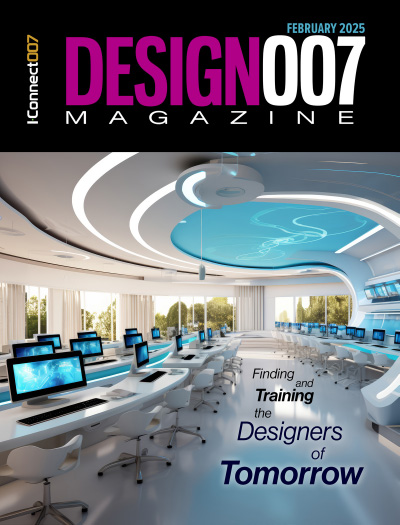
Training New Designers
Where will we find the next generation of PCB designers and design engineers? Once we locate them, how will we train and educate them? What will PCB designers of the future need to master to deal with tomorrow’s technology?

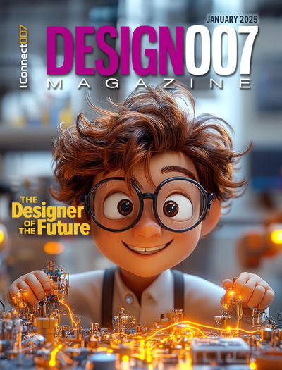
The Designer of the Future
Our expert contributors peer into their crystal balls and offer their thoughts on the designers and design engineers of tomorrow, and what their jobs will look like.
- Articles
- Columns
Search Console
- Links
- Media kit
||| MENU - design007 Magazine
Here’s Looking at You, Kid
February 13, 2025 | IPC Community Editorial TeamEstimated reading time: 1 minute
Our industry is facing a two-fold challenge: finding the next generation of PCB designers and training these young technologists. Most high school career counselors don't know anything about this career, and electrical engineering grads leave college with little or no PCB design knowledge. Where do we start?
We asked two PCB design instructors, IPC’s Kris Moyer and Palomar College’s John Watson, to weigh in on the best methods for finding and training the designers of tomorrow.
Andy Shaughnessy: Gentlemen, as PCB design instructors, you have front-row seats to what’s going on, so, how can we find and train the next generation of PCB designers?
John Watson: We have a weeklong program at Palomar College that takes place in the high schools where the kids get to work on an actual PCB design. Next week we are visiting two high schools in the San Diego area. It definitely is something I hope to expand on, depending on who wants to pick up that sort of program. The first step is to get them to notice when they are young. There are a lot of intelligent kids in high school who are very intuitive, and they pick this up very quickly.
Kris Moyer: Yes, I agree. We also need them to see that PCB design is an actual engineering discipline. When I was in high school, I was looking for my path to engineering, but part of our problem today is we have not defined board designers as “board engineers.” We have to show that this is a desirable, cutting-edge job. We have to introduce the narrative earlier and change that narrative to engineering.
To read this entire conversation, which appeared in the February 2025 issue of Design007 Magazine, click here.
Suggested Items
Real Time with... IPC APEX EXPO 2025: New Dispensing and Coating Solutions
04/03/2025 | Real Time with...IPC APEX EXPOMichael Hanke, Global Sales Officer at Rehm, discusses new dispensing and coating equipment developed in Germany. He emphasizes the significance of software integration with customer systems to tackle market challenges.
Real Time with... IPC APEX EXPO 2025: Maximizing Cost Savings in PCB Design With NCAB
04/02/2025 | Real Time with...IPC APEX EXPOKelly Dack and Lonnie Port discuss NCAB's role in the printed circuit board industry. With 30 years of experience, NCAB emphasizes the importance of customer involvement during the design process to achieve significant cost reductions.
'Let’s Talk Production Test' with Bert Horner of The Test Connection, Inc. at SMTA Long Island Meeting
04/02/2025 | The Test Connection Inc.The Test Connection Inc. (TTCI), a leading provider of electronic test and manufacturing solutions, is pleased to announce that its President, Bert Horner, will present at the SMTA Long Island Chapter Technical Meeting & Dinner on Wednesday, April 16, 2025. The event will take place at the Radisson Hotel Hauppauge in Hauppauge, NY.
CEE PCB Appoints Markus Voeltz to Business Development Director Europe
04/02/2025 | CEE PCBCEE PCB, a leading manufacturer of printed circuit boards (PCBs) and flexible printed circuits (FPCs) with 3 production facilities in China, is expanding its presence in Europe and began providing local support in March 2025. With 25 years of experience in the industry, the company is enhancing its commitment to European customers by providing more direct collaboration for technical inquiries and advice.
BEST Inc. Presents StencilQuik for Simplifying BGA Rework Challenges
04/02/2025 | BEST Inc.BEST Inc., a leader in electronic component rework services, training, and rework tools is thrilled to announce StencilQuik™ rework stencils. This innovative product is specifically designed for placing Ball Grid Arrays (BGAs) or Chip Scale Packages (CSPs) during the rework process.


