


 The Shaughnessy Report: A Plan for Floor Planning
 Dana on Data: Best Practices in Interpreting Drawing Notes—‘Use Latest Revision’
 Connect the Dots: Sequential Lamination in HDI PCB Manufacturing


AT&S Starts Construction of First High-tech Manufacturing Facility in Southeast Asia
October 29, 2021 | AT&SEstimated reading time: 2 minutes
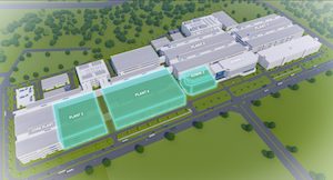
AT&S, one of the globally leading manufacturers of high-end printed circuit boards and IC substrates, headquartered in Austria (Europe), announced detailed project information on the company’s planned investment in a state-of-the-art factory for IC substrates at the Kulim Hi-Tech Park, Kedah.
During a press conference, AT&S CEO Andreas Gerstenmayer and AT&S COO Ingolf Schroeder gave insights into the planned investment, the project scope, technology details, as well as the planned activities to hire approx. 6,000 highly qualified employees.
AT&S’ new campus for the production of IC substrates in Kulim Hi-Tech Park, Kedah, involves a proposed total investment for phase 1 of RM 8.5 billion (€1.7 billion). The construction of the facility is going to start with an official groundbreaking ceremony on October 30, 2021, with commercial operations targeted to come on stream in 2024.
“I want to thank the Malaysian government as well as the MIDA (the government’s principal promotion agency under the Ministry of International Trade and Industry) for the great support throughout the entire process, from the start of our location scouting until today,” says AT&S CEO Andreas Gerstenmayer. “Already today, Malaysia is an important hub for the chip supply chain. We are convinced that Malaysia can further strengthen its position as a technology country and will develop its position in the region as a high-tech manufacturing hub in Asia,” Gerstenmayer says.
Not only will thousands of new jobs be created in the region, but Malaysia will make a name for itself as a hotspot for a completely new, first-of-its-kind technology segment. “AT&S brings the latest generation of high-end technologies to Malaysia and will establish a completely new technology sector in one of the future global microelectronic hotspots. In addition to manufacturing high-tech products, extensive R&D activities will also be conducted at this new site,” AT&S COO Ingolf Schroeder says.
All these activities require a high amount of highly qualified human resources and will boost the region’s labor market. The search profiles for employees at the new AT&S plant range from specialists, managers, and leaders in the areas of electronic, mechanical, and chemical engineers, and business. At the same time, AT&S is also looking for about 4,500 blue-collar workers who can work in a highly sophisticated shop floor environment.
Besides manufacturing, R&D will also be a focus at the new AT&S facility in Kulim. Therefore, AT&S is investigating cooperation and partnerships with leading universities in Malaysia. “These partnerships will not only help us to discover new paths for the microelectronics industry,” Andreas Gerstenmayer says. “They will also make an important contribution to the development of extensive know-how in the various areas of the microelectronics industry for Malaysia and, at the end of the day, contribute to the positive development of the society.”
Share on:


Testimonial
"Advertising in PCB007 Magazine has been a great way to showcase our bare board testers to the right audience. The I-Connect007 team makes the process smooth and professional. We’re proud to be featured in such a trusted publication."
Klaus Koziol - atgSuggested Items
MKS’ Atotech to Participate in IPCA Electronics Expo 2025
08/11/2025 | AtotechMKS Inc., a global provider of enabling technologies that transform our world, announced that its strategic brands ESI® (laser systems) and Atotech® (process chemicals, equipment, software, and services) will showcase their latest range of leading manufacturing solutions for printed circuit board (PCB) and package substrate manufacturing at the upcoming 17th IPCA Show to be held at Pragati Maidan, New Delhi from August 21-23, 2025.
EMC-Taiwan Announces Further Investment in North America
08/11/2025 | Elite Material Co. LtdElite Material Company (EMC)-Taiwan announced that it has made a commitment to invest $80 million dollars in the Arlon EMD factory in Rancho Cucamonga, CA it acquired at the end of 2020.
I-Connect007 Editor’s Choice: Five Must-Reads for the Week
08/08/2025 | Andy Shaughnessy, I-Connect007If you’ve been watching the news lately, you might be tempted to opine, “What’s going on here?” In this week’s must-reads, we have a wrap-up of the latest news about U.S. tariffs with Asia, and columnist Tom Yang explains why some PCB fabrication business should remain in China. We also have a piece that examines the unprecedented growth that green manufacturing is expected to see over the next four years.
Materials and Manufacturing for the AI Era: The Next PCB Frontier
08/08/2025 | Edy Yu, Chief Editor, ECIO, and the I-Connect007 Editorial TeamAI is pushing hardware to its limits, and the bottleneck isn’t design anymore—it’s materials. Next-generation AI servers aren’t just heavier on layer counts. They demand better materials to handle the speed, heat, and signal integrity requirements of 400G, 800G, and even 1.6T Ethernet systems. Many server motherboards are already 32–36 layers. For the next wave of 1.6T-capable boards, expect 40–50 layers, which must maintain high-frequency performance without degrading signal quality.
Nvidia’s PCB Vendor Victory Giant Plans to Raise Funds in Hong Kong IPO
08/07/2025 | I-Connect007 Editorial TeamNvidia supplier Victory Giant Technology, based in Huizhou, Guangdong, China, released plans at the end of July for a Hong Kong share offering. The move came after regulators eased fundraising rules to support high-tech companies, the South China Morning Post reported.