


 Fresh PCB Concepts: Resilience and Renewal in Domestic PCB Manufacturing
 Designers Notebook: Power and Ground Distribution Basics
 Elementary, Mr. Watson: Heat—The Hidden Villain of Power Electronics


BEST Inc. Introduces StikNPeel Rework Stencil for Fast, Simple and Reliable Solder Paste Printing
June 2, 2025 | BEST Inc.Estimated reading time: 1 minute
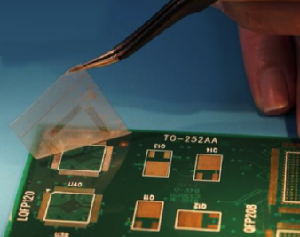
BEST Inc., a leader in electronic component rework services, training, and products is pleased to introduce StikNPeel™ rework stencils. This innovative product is designed for printing solder paste for placement of gull wing devices such as quad flat packs (QFPs) or bottom terminated components.
StikNPeel™ simplifies the process of selectively printing solder paste onto a printed circuit board. The process is as simple as peeling off the stencil backing, aligning in the proper location, and placing the stencil on the circuit board pad site. The StikNPeel™ stencil is secured in place on the PCB via a repositionable adhesive backing. Once properly placed, solder paste is dispensed across the stencil to obtain sufficient solder paste deposition. Next, the StikNPeel™ stencil is peeled off the circuit board leaving uniform solder paste volume in the aperture areas without any remaining residues or visible signs of rework. Once the stencil is removed, you’re ready for component placement.
Using StikNPeel™ stencils streamlines component placement without the common issues and mess that come with using metal stencils. The flexible material and adhesive backing ensure the board and stencil remain coplanar, preventing solder paste smearing and improving first-pass yields. Once aligned and pressed into place, the stencil remains adhered to the board providing uniform solder paste distribution. Utilizing this process eliminates the need for time-consuming masking around the rework area. Additionally, the StikNPeel™ stencil can be equipped with peripheral flaps to allow tighter positioning when navigating neighboring devices. Compared to our stay-in-place stencils, StikNPeel™ is removed from the board prior to component placement and leaves no visible evidence of rework.
StikNPeel™ rework stencils are custom made to your exact device requirements without the need for expensive tooling. One pack consists of 10 stencils in a pink anti-static bag. No minimum order requirements apply. Typical lead time is 3-5 days for up to 4 packs after check plot approval. Approved files include Gerber, DXF, or component mechanical specs.
Share on:


Testimonial
"Your magazines are a great platform for people to exchange knowledge. Thank you for the work that you do."
Simon Khesin - Schmoll MaschinenSuggested Items
Federal Electronics Enhances Hermosillo Operations with Installation of Mycronic MyPro S30 Stencil Printer
09/29/2025 | Federal ElectronicsFederal Electronics, a leader in providing advanced electronic manufacturing services, has expanded its production capabilities with the installation of a new Mycronic MyPro S30 Stencil Printer at its Hermosillo facility.
Secure Semiconductor Manufacturing Acquires Full SMT Line from Manncorp
09/11/2025 | ManncorpSecure Semiconductor Manufacturing, LLC (SSM), an American-owned company dedicated to producing secure printed wiring boards and advanced assembly solutions in the MidWest USA, today announced the acquisition of a complete surface mount technology (SMT) line from Manncorp.
AQUANOX A4618 and CYBERSOLV C8882 to Lead KYZEN Offerings at SMTA Long Island Expo and Tech Forum
08/27/2025 | KYZEN'KYZEN, the global leader in innovative environmentally responsible cleaning chemistries, will exhibit at the SMTA Long Island Expo & Tech Forum on Wednesday, Sept. 10, 2025 at the Marriott Melville Long Island.
KYZEN to Feature CYBERSOLV 141-K and KYZEN E5631J at SMTA Michigan Expo and Tech Forum
08/05/2025 | KYZEN'KYZEN, the global leader in innovative environmentally responsible cleaning chemistries, will exhibit at the SMTA Michigan Expo and Tech Forum, scheduled to take place Tuesday, August 19, 2025 at Laurel Manor in Livonia, Michigan. During the event, the KYZEN Clean Team will highlight precision aerosol cleaner CYBERSOLV 141-K and understencil cleaner KYZEN E5631J.
KYZEN to Focus on Aqueous Cleaning and Stencil Cleaning at SMTA Juarez
05/20/2025 | KYZEN'KYZEN, the global leader in innovative environmentally responsible cleaning chemistries, will exhibit at the SMTA Juarez Expo and Tech Forum, scheduled to take place Thursday, June 5 at the Injectronics Convention Center in Ciudad Jarez, Chihuahua.