


 Fresh PCB Concepts: Resilience and Renewal in Domestic PCB Manufacturing
 Designers Notebook: Power and Ground Distribution Basics
 Elementary, Mr. Watson: Heat—The Hidden Villain of Power Electronics


TSI Introduces the Nano LPM System for Semiconductor Ultrapure Water Nanoparticle Detection
March 14, 2025 | TSI IncorporatedEstimated reading time: 1 minute
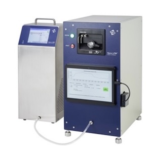
TSI Incorporated, a global leader in precision measurement and data-driven solutions, announces the introduction of the new TSI Nano LPM™ System, marking a breakthrough in ultrapure water (UPW) monitoring for the semiconductor industry, and solving the problem of detecting particles down to a level that has never been done before. The Nano LPM™ System delivers true 10 nanometer (nm) nanoparticle detection, providing a continuous, reliable monitoring of UPW quality. This innovation empowers semiconductor manufacturers to make real-time, data-driven decisions before product quality and yield is affected.
In semiconductor manufacturing, UPW is integral for tasks such as wafer and equipment cleaning, etching, and contaminant removal, directly impacting production quality. Particles as small as 10 nm can compromise yield, making real-time detection a vital need. Traditional optical technologies have struggled detecting nanoparticles below 20 nm due to refractive index limitations and interference from microbubbles, often resulting in inconsistent or inaccurate readings. TSI’s Nano LPM™ System tackles these limitations with a patented approach that ensures accurate detection of particles at 10 nm, giving semiconductor facilities a robust and consistent monitoring tool.
The Nano LPM™ System sets a new standard in UPW nanoparticle monitoring with its Nano LPM Particle Generator, that aerosolizes UPW, effectively drying droplets and isolating solid nanoparticles. These nanoparticles are then analyzed using the Nano LPM Water-Based Condensation Particle Counter (CPC), optimized for cleanroom environments.
“TSI’s Nano LPM™ System represents a significant leap forward for semiconductor manufacturers who need reliable, real-time UPW monitoring at the 10 nm level,” said Ketan Mehta, VP of Product Management and Marketing at TSI. “We’re proud to offer a groundbreaking technology that not only ensures compliance but also elevates product quality and yield, transforming environmental control into a critical advantage for our customers.”
Share on:


Testimonial
"We’re proud to call I-Connect007 a trusted partner. Their innovative approach and industry insight made our podcast collaboration a success by connecting us with the right audience and delivering real results."
Julia McCaffrey - NCAB GroupSuggested Items
LPMS USA Named the Authorized National Distributor for Henkel Printed Electronics Inks and Coatings
03/05/2025 | LPMS USALPMS USA, a leader in low pressure molding solutions, is proud to announce they have been named the authorized national distributor for Henkel printed electronics inks and coatings.
LPMS USA to Offer Live Molding Demos at IPC APEX 2025
02/07/2025 | LPMS USALPMS USA, a leader in low pressure molding solutions, is thrilled to exhibit at IPC APEX 2025. Join us at Booth #2300 for live molding demonstrations using the innovative KAPPA 1100H.
Henkel Forms Partnership with LPMS USA
09/22/2015 | HenkelIn a move designed to offer customers greater access to low pressure molding solutions and its award-winning TECHNOMELT materials, Henkel Adhesive Technologies has formed a partnership with leading molding equipment manufacturer, LPMS USA.