-

- News
- Books
Featured Books
- design007 Magazine
Latest Issues
Current Issue
Training New Designers
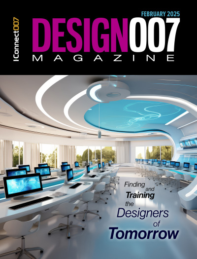
Where will we find the next generation of PCB designers and design engineers? Once we locate them, how will we train and educate them? What will PCB designers of the future need to master to deal with tomorrow’s technology?

The Designer of the Future
Our expert contributors peer into their crystal balls and offer their thoughts on the designers and design engineers of tomorrow, and what their jobs will look like.

Advanced Packaging and Stackup Design
This month, our expert contributors discuss the impact of advanced packaging on stackup design—from SI and DFM challenges through the variety of material tradeoffs that designers must contend with in HDI and UHDI.
- Articles
- Columns
Search Console
- Links
- Media kit
||| MENU - design007 Magazine
TTM’s Grand Opening in Malaysia
November 7, 2024 | Marcy LaRont, I-Connect007Estimated reading time: 2 minutes
When I last spoke with Tom Edman, president and CEO of TTM Technologies (TTM), he provided an update about the company’s new high-tech printed circuit board facility under construction in Syracuse, New York, and how the grand opening of a facility in Malaysia is informing TTM’s overall expansion efforts: a cutting-edge facility spread across 27 acres and providing roughly 1,000 jobs. Now, Tom provides more details about the new automated facility, its regional and global impact, and the importance of having both government and industry support.
Marcy LaRont: Tom, tell me about TTM Malaysia.
Tom Edman: TTM Malaysia is a slightly more than 800,000-square-foot building with a single-level production floor, which allows us to incorporate a high degree of automation. For example, we're combining process steps to accommodate automation using inline equipment when and where we can and between process steps as well. We're also using automated guided vehicles (AGVs) to transport panels. Almost everything inside the facility is automated, including the drills and the drill bit sharpening. That might sound mundane, but it is a very important part of the process in terms of keeping the drill points properly calibrated. We have a large facility just above the production floor where we feed chemistry onto the first floor, and we have a sub-basement for taking the waste which delivers the spent water and chemistry to the adjacent waste treatment center for recycling or treatment.
LaRont: Automation is certainly key, so tell me more about the AGVs.
Edman: They move the panels around from the warehouse to the loaders, between the pieces of equipment for each process step, and finally back to the warehouse. You can see these little robots all over the facility.
We incorporated manufacturing execution system (MES) software to dictate their movements. This software runs the shop floor processes and ties into our Oracle® financial system. As we proceed through the ramp-up, this last step toward automation allows us to minimize scrap because we have eliminated manual handling errors.
We have a very long hallway that runs lengthwise throughout the middle of the facility for evacuation purposes. We put in doors with glass panels so visitors can get a good feeling for the entire process. As you move your way through the different process steps, you see drill, plating, test and inspection, and finally return to where you started.
To read this entire conversation, which appeared in the October 2024 issue of PCB007 Magazine, click here.
Suggested Items
FTG Announces New Aerospace Facility in Hyderabad, India
02/12/2025 | Firan Technology GroupFiran Technology Group Corporation announced the establishment of a new aerospace operation in Hyderabad, India, set to start production by the end of 2025.
3M Joins Consortium to Accelerate Semiconductor Technology in the U.S.
02/04/2025 | PR Newswire3M is expanding its commitment to the semiconductor industry by joining the US-JOINT Consortium, a strategic partnership of 12 leading semiconductor suppliers. The consortium drives research and development in next-generation semiconductor advanced packaging and back-end processing technologies anchored by a new cutting-edge facility in Silicon Valley.
U.S. Navy Awards Lockheed Martin $383M for Next Generation of U.S. Deterrence at Sea
02/04/2025 | Lockheed MartinThe U.S. Navy awarded Lockheed Martin a $383 million cost-plus-incentive-fee and cost-plus-fixed-fee modification to the existing Lockheed Martin contract for development of the next generation of the Trident II Strategic Weapons System (SWS) D5 missile to continue the nation's sea-based strategic deterrence.
FTG Completes New Banking Agreement
01/31/2025 | Globe NewswireFiran Technology Group Corporation announced that is has completed a new 3-year banking agreement with BMO Corporate Finance, which matures December 11, 2027.
ElectroCraft Expands Ann Arbor Facility to Strengthen U.S. Manufacturing Independence and Reduce Lead Times
01/31/2025 | PRNewswireElectroCraft, a global leader in motor and motion control solutions, proudly announces the significant expansion of its Ann Arbor, Michigan facility.


