


 Elementary, Mr. Watson From Classroom to Career—Bridging the Gap in PCB Design Talent
 Global PCB Connections: How Technology Can Level the Playing Field
 Fresh PCB Concepts: Traceability in PCB Design


Researchers Realize World’s Thinnest Optical Hologram with 2-D Material Monolayer
August 22, 2019 | Missouri S&TEstimated reading time: 2 minutes
Missouri S&T researchers are demonstrating a new concept to reconstruct holographic images by using a single two-dimensional material monolayer with the thickness of less than one nanometer. Their work could lead to the creation of smart watches with holographic displays, printed security cryptograms on bank notes and credit cards, and new possibilities for data storage.
The researchers describe their atomically thin nonlinear optical holograms in Nano Letters, one of the top journals in nanotechnology research, and prototype their device by reconstructing several kinds of holographic images with tungsten disulfide monolayers of the thickness of around 0.7 nanometer. A nanometer is one billionth of a meter, and a tungsten disulfide monolayer only contains one layer of tungsten atoms sandwiched between two layers of sulfur atoms.
The approach is described in the Nano Letters paper “Atomically thin nonlinear transition metal dichalcogenide holograms,” which was published online Friday, Aug. 16. It involves the use of only a single nanopatterned tungsten disulfide monolayer that is able to control the wavefront of light, where the designed hologram patterns are punctured by a nanofabrication process known as focused ion beam milling.
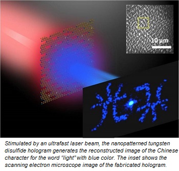
Experimenting with the ultrafast laser excitation on the nanopatterned tungsten disulfide monolayer, the researchers demonstrated a nonlinear optical hologram with high conversion efficiency and atomic thickness, for producing optical vortex beams and Airy beams as well as reconstructing complex holographic images at the second harmonic frequency. An Airy beam is a waveform that appears to curve as it moves.
In their paper, the Missouri S&T researchers published reconstructed holographic images of the Chinese character for the word “light” with blue and green colors. They believe this new type of optical hologram holds promise for future applications, such as security markings on banknotes and credit cards, optical communications, smart watch displays, and data storage.
“We are able to control the binary amplitude modulation of zero and one by simply etching out or keeping the tungsten disulfide monolayer area,” says Dr. Xiaodong Yang, an associate professor in mechanical and aerospace engineering at Missouri S&T. “Our holograms possess significantly higher nonlinear conversion efficiency than the currently existing plasmonic metasurface holograms made of metallic nanostructures.”
“In addition, our holograms have atomic thickness of less than one nanometer, much thinner than the usual thickness of tens of nanometers for plasmonic metasurfaces and several hundred nanometers for dielectric metasurfaces,” says Dr. Jie Gao, an associate professor of mechanical and aerospace engineering at Missouri S&T and co-author of the paper.
Share on:


Suggested Items
Real Time with... IPC APEX EXPO 2025: Navigating Aerospace Training Trends With Blackfox
02/26/2025 | Real Time with...IPC APEX EXPOSharon Montana-Beard, Blackfox Training’s vice president of international and strategic sales, updates Nolan Johnson on the latest training demands and offerings from Blackfox.
Incap UK Installs Vertical Storage System to Optimise PCBA Management
02/24/2025 | IncapIncap UK installed two vertical storage systems to enhance PCBA (Printed Circuit Board Assembly) storage, boosting efficiency, accuracy, and order fulfilment speed. The investment is expected to improve stock handling efficiency by at least 40%.
Summit Interconnect Welcomes Leo LaCroix as Vice President of Aerospace & Defense Operations
02/21/2025 | Summit Interconnect, Inc.Summit Interconnect, a leading provider of advanced printed circuit board (PCB) solutions, is pleased to announce that Leo LaCroix has joined the company as Vice President of Aerospace & Defense Operations. In this role, LaCroix will oversee operational strategy, customer engagement, and manufacturing excellence for Summit’s aerospace and defense-focused facilities, driving continued growth and innovation in the sector.
FTG Announces Full Year and Q4 2024
02/20/2025 | Firan Technology Group CorporationDuring 2024, the Corporation invested in existing sites and grew the business organically. FTG is strategically deploying its capital in ways that will drive increased shareholder returns for the future in both the near term and long term. Specifically, FTG accomplished many goals in 2024 that continue to improve the Corporation and position it for the future, including:
FTG Announces New Aerospace Facility in Hyderabad, India
02/12/2025 | Firan Technology GroupFiran Technology Group Corporation announced the establishment of a new aerospace operation in Hyderabad, India, set to start production by the end of 2025.