


 Target Condition: Distribution of Power—Denounce the Ounce
 Fresh PCB Concepts: Resilience and Renewal in Domestic PCB Manufacturing
 Designers Notebook: Power and Ground Distribution Basics


Partnership to Develop an All-Perovskite Solar Cell
September 27, 2018 | Oxford PVEstimated reading time: 1 minute
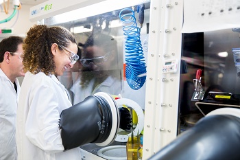
Oxford PV, The Perovskite Company, the leader in the field of perovskite solar cells, announced a five year research project with the University of Oxford to develop a thin-film multi-junction perovskite solar cell, with a target 37% efficiency and long term stability.
The £5 million collaboration has been awarded £2.5 million from the Engineering and Physical Sciences Research Council (EPSRC) as part of its Prosperity Partnerships programme, with the remainder matched by Oxford PV. The EPSRC grant is designed to support long term, research-based partnerships between business and universities, with national and global importance.
From the University of Oxford, both the Photovoltaic and Optoelectronic Device Research Group led by Professor Henry Snaith (Oxford PV’s Chief Scientific Officer and Co-founder), and the Semiconductor Research Group led by Professor Laura Herz, will form the partnership with Oxford PV.
Dr. Chris Case, chief technology officer at Oxford PV commented, “Oxford PV’s commercial focus remains firmly on its two-terminal perovskite-on-silicon tandem solar cell technology. We have made significant progress in this respect. Today, commercial sized perovskite-on-silicon tandem solar cells are in production at our pilot line and we are optimising equipment and processes in preparation for commercial deployment.
“Oxford PV is always exploring new ways to push the boundaries in perovskite solar cell technology development—this new initiative with Oxford University is one such project. Longer term, providing the PV industry with a low cost solar cell technology that could reach an efficiency level of nearly 40%, is an exciting prospect that would further transform global solar energy generation—helping drive the world toward an all-electric future.”
In June, Oxford PV set a world record certified efficiency of 27.3% for its perovskite-on-silicon solar cell. This exceeded the 26.7% efficiency world record for a single junction silicon solar cell – further validating the ability of perovskite to enhance the performance of silicon-based photovoltaics. Oxford PV’s perovskite-on-silicon solar cell technology roadmap extends beyond 30% efficiency.
Share on:


Testimonial
"Our marketing partnership with I-Connect007 is already delivering. Just a day after our press release went live, we received a direct inquiry about our updated products!"
Rachael Temple - AlltematedSuggested Items
GlobalFoundries, Silicon Labs Expand Partnership to Accelerate Wireless Connectivity Solutions and Strengthen U.S. Chip Manufacturing
11/05/2025 | GlobalFoundriesGlobalFoundries (GF), one of the world’s leading semiconductor manufacturers, and Silicon Labs, the leading innovator in low-power wireless, announced the expansion of their strategic partnership to advance the development of next-generation, energy-efficient wireless technologies and scale U.S.-based semiconductor manufacturing.
Learning With Leo: UHDI—The Next Leap in PCB Manufacturing
11/05/2025 | Leo Lambert -- Column: Learning With LeoHigh density interconnect (HDI) technology has been a cornerstone of miniaturized electronics since Hewlett-Packard introduced the first chip-scale implementation in 1982. Over time, HDI processes became central to organic flip-chip packaging in the semiconductor industry. Today, the convergence of IC substrates and system-level PCBs has accelerated the adoption of UHDI.
On the Line With… Ultra HDI, Episode 8: “Materials, Up and Coming Capabilities,” Now Available
11/05/2025 | I-Connect007I-Connect007 is excited to announce the release of the eighth episode of its 12-part podcast series, On the Line With… American Standard Circuits: Ultra HDI. In this episode, “Materials, Up and Coming Capabilities,” host Nolan Johnson sits down with resident expert John Johnson, Director of Quality and Advanced Technology at American Standard Circuits, to discuss how material selection influences the Ultra HDI (UHDI) manufacturing process.
High Density Packaging User Group Announces ASKPCB Membership
11/03/2025 | HDP User GroupHigh Density Packaging User Group (HDP) is pleased to announce that the Aoshikang Technology (Hong Kong) Co., Ltd (ASKPCB) has become a member.
Cephia Secures $4M Seed Funding to Revolutionize Multimodal Sensing with Metasurface Technology
10/31/2025 | PRNewswireCephia, a startup building products using advanced AI computational imaging technologies and silicon sensors made from advanced metamaterials, formally launched with several pilot customers and $4 million in seed venture capital funding.