


 Target Condition: Distribution of Power—Denounce the Ounce
 Fresh PCB Concepts: Resilience and Renewal in Domestic PCB Manufacturing
 Designers Notebook: Power and Ground Distribution Basics


Funding for Preparing Perovskite Solar Cells for High Volume Manufacturing
August 24, 2018 | HZBEstimated reading time: 1 minute
HZB participates in a new consortium for Perovskite solar technology that is led by Oxford PV Germany GmbH. The consortium is funded by the German Ministry of Economics and Energy with 2.8 Million Euros and aims to further demonstrate the manufacturability of perovskite-silicon tandem solar cells.
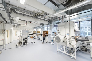
Image Caption: View into the new HySPRINT laboratory at HZB, where perovskit solar cells can be produced and tested. Photo: HZB/M. Setzpfandt
Further partners are Von Ardenne GmbH, Fraunhofer-Institute for Solar Energy Systems ISE, and the Technical University of Berlin. The project will focus on preparing perovskite solar cell technology for high volume manufacturing. This will include the optimisation of the perovskite-silicon tandem solar cell architecture, to make further efficiency improvements on industrial 156 mm x 156 mm wafer formats; the refinement of industrial scale process technology; and life-cycle analysis to inform the social-environmental impact of the tandem solar cells.
"Perovskite-based tandem solar cells are very promising to achieve really high efficiencies. In order to contribute to this exciting development we have built up strong competences in perovskites and tandem cell technology such as the Helmholtz Innovation Lab HySPRINT", says Prof. Dr. Rutger Schlatmann, Director of the Competence Center Thin Film and Nanotechnology for Photovoltaics Berlin (PVcomB) at HZB. "To the consortium with Oxford PV, we contribute our vast expertise in high-efficiency silicon heterojunction bottom cells", adds Dr. Bernd Stannowski who is leading these activities at the PVcomB.
Dr. Chris Case, Chief Technology Officer at Oxford PV says “The consortium partners bring together the perfect balance of expertise. Refining the manufacturing process of our perovskite solar cell technology will ensure the highest performing tandem solar cell in the field and the easy transfer of our technology into silicon solar cell and module production lines.”
In June 2018, HZB and Oxford achieved an independently certified efficiency of 25.2 % for their perovskite silicon tandem solar cell. “In our cooperation, we aim to further optimize perovskite silicon tandem cells, demonstrate their scalability and facilitate their integration into large-area solar modules”, says Rutger Schlatmann.
Share on:


Testimonial
"Advertising in PCB007 Magazine has been a great way to showcase our bare board testers to the right audience. The I-Connect007 team makes the process smooth and professional. We’re proud to be featured in such a trusted publication."
Klaus Koziol - atgSuggested Items
GlobalFoundries, Silicon Labs Expand Partnership to Accelerate Wireless Connectivity Solutions and Strengthen U.S. Chip Manufacturing
11/05/2025 | GlobalFoundriesGlobalFoundries (GF), one of the world’s leading semiconductor manufacturers, and Silicon Labs, the leading innovator in low-power wireless, announced the expansion of their strategic partnership to advance the development of next-generation, energy-efficient wireless technologies and scale U.S.-based semiconductor manufacturing.
Learning With Leo: UHDI—The Next Leap in PCB Manufacturing
11/05/2025 | Leo Lambert -- Column: Learning With LeoHigh density interconnect (HDI) technology has been a cornerstone of miniaturized electronics since Hewlett-Packard introduced the first chip-scale implementation in 1982. Over time, HDI processes became central to organic flip-chip packaging in the semiconductor industry. Today, the convergence of IC substrates and system-level PCBs has accelerated the adoption of UHDI.
On the Line With… Ultra HDI, Episode 8: “Materials, Up and Coming Capabilities,” Now Available
11/05/2025 | I-Connect007I-Connect007 is excited to announce the release of the eighth episode of its 12-part podcast series, On the Line With… American Standard Circuits: Ultra HDI. In this episode, “Materials, Up and Coming Capabilities,” host Nolan Johnson sits down with resident expert John Johnson, Director of Quality and Advanced Technology at American Standard Circuits, to discuss how material selection influences the Ultra HDI (UHDI) manufacturing process.
High Density Packaging User Group Announces ASKPCB Membership
11/03/2025 | HDP User GroupHigh Density Packaging User Group (HDP) is pleased to announce that the Aoshikang Technology (Hong Kong) Co., Ltd (ASKPCB) has become a member.
Cephia Secures $4M Seed Funding to Revolutionize Multimodal Sensing with Metasurface Technology
10/31/2025 | PRNewswireCephia, a startup building products using advanced AI computational imaging technologies and silicon sensors made from advanced metamaterials, formally launched with several pilot customers and $4 million in seed venture capital funding.