


 Elementary, Mr. Watson From Classroom to Career—Bridging the Gap in PCB Design Talent
 Global PCB Connections: How Technology Can Level the Playing Field
 Fresh PCB Concepts: Traceability in PCB Design


Akrometrix Launches New Warpage Metrology System
June 29, 2017 | Akrometrix LLCEstimated reading time: 1 minute
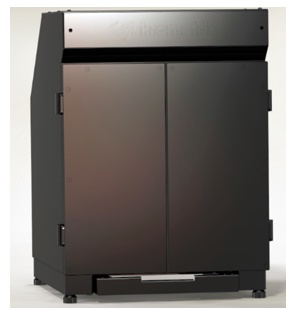
Akrometrix, LLC, the leading provider of thermal warpage and strain metrology equipment to both the front- and back-end semiconductor and electronics industries, is pleased to announce that it has launched its newest warpage metrology system – the Tabletop Shadow Moiré (TTSM) system.
“Over the years, many of our customers who are using our systems for thermal warpage metrology have stated a need for an ultra-fast, highly accurate room temperature warpage metrology system,” stated Mayson Brooks, Akrometrix President. “Additionally, they wanted a system that was small enough for a tabletop operation and that would allow them to utilize all the software features of our thermal warpage systems, only at room temperature.”
The TTSM meets this demand – enabling customers to measure warpage of substrates up to 300mm x 310 mm (a 300mm wafer or two JEDEC trays) with the entire measurement taking less than two seconds. Whether individual parts or a JEDEC tray of multiple parts, the TTSM provides an ultra-fast and highly accurate measurement at room temperature that is suited for tabletop use.
About Akrometrix LLC
Akrometrix is the leader in thermal warpage and strain metrology for the front-end/back-end wafer, back-end packaging/assembly, panel and the PCB/component markets. The company provides both capital equipment and test services to measure warpage and strain in temperatures from -50°C to 300°C on virtually any substrate up to 600mm x 600mm, regardless of shape. Located in Atlanta, Georgia, Akrometrix has been serving customers worldwide for more than 20 years based on technology developed at Georgia Tech. For more information click here.
Share on:


Suggested Items
OMRON Partners with Wiferion for Inductive AMR Charging
02/28/2025 | OmronWorking together to increase the performance of autonomous mobile robots (AMRs) and enable new application concepts — to achieve this goal, OMRON has certified Wiferion’s wireless charging technology for the LD series robots.
Variosystems Acquires Heicks Industrieelektronik; Strengthens Aerospace Expertise and Expands Presence in Germany
02/28/2025 | Variosystems AGVariosystems has acquired Heicks Industrieelektronik GmbH, a leading technology company specializing in electronic solutions for the aerospace sector, and will fully integrate it into the Variosystems Group.
Lockheed Martin Unveils Scalable Counter-Unmanned Aerial System Solution
02/28/2025 | Lockheed MartinAs the threat of small Unmanned Aerial Systems (UAS) continues to evolve, Lockheed Martin (NYSE: LMT) is demonstrating a new approach to counter these emerging threats.
eInfochips Joins Samsung Advanced Foundry Ecosystem (SAFE™) to Drive Semiconductor Innovation
02/28/2025 | PRNewswireeInfochips, an Arrow Electronics company, announced the company has joined the Samsung Advanced Foundry Ecosystem (SAFE™) as a Virtual Design Partner.
PsiQuantum Announces Omega, a Manufacturable Chipset for Photonic Quantum Computing
02/27/2025 | BUSINESS WIREPsiQuantum announces Omega, a quantum photonic chipset purpose-built for utility-scale quantum computing. Featured in a newly published paper in Nature, the chipset contains all the advanced components required to build million-qubit-scale quantum computers and deliver on the profoundly world-changing promise of this technology.