


















 Elementary, Mr. Watson: Waking Up Europe's PCB Giants
 Connect the Dots: Getting the PCB Quote Right
 Powering the Future: What Engineers Get Wrong About Designing for Reliability





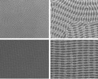
Since the 1960s, computer chips have been built using a process called photolithography. But in the past five years, chip features have gotten smaller than the wavelength of light, which has required some ingenious modifications of photolithographic processes. Keeping up the rate of circuit miniaturization that we’ve come to expect — as predicted by Moore’s Law — will eventually require new manufacturing techniques.
Block copolymers, molecules that spontaneously self-assemble into useful shapes, are one promising alternative to photolithography. In a new paper in the journal Nature Communications, MIT researchers describe the first technique for stacking layers of block-copolymer wires such that the wires in one layer naturally orient themselves perpendicularly to those in the layer below.
The ability to easily produce such “mesh structures” could make self-assembly a much more practical way to manufacture memory, optical chips, and even future generations of computer processors.
“There is previous work on fabricating a mesh structure — for example our work,” says Amir Tavakkoli, a postdoc in MIT’s Research Laboratory of Electronics and one of three first authors on the new paper. “We used posts that we had fabricated by electron-beam lithography, which is time consuming. But here, we don’t use the electron-beam lithography. We use the first layer of block copolymer as a template to self-assemble another layer of block copolymer on top of it.”
Tavakkoli’s co-first-authors on the paper are Sam Nicaise, a graduate student in electrical engineering, and Karim Gadelrab, a graduate student in materials science and engineering. The senior authors are Alfredo Alexander-Katz, the Walter Henry Gale Associate Professor of Materials Science and Engineering; Caroline Ross, the Toyota Professor of Materials Science and Engineering; and Karl Berggren, a professor of electrical engineering.
Page 1 of 3
Share on:


Testimonial
"We’re proud to call I-Connect007 a trusted partner. Their innovative approach and industry insight made our podcast collaboration a success by connecting us with the right audience and delivering real results."
Julia McCaffrey - NCAB GroupSuggested Items
What Climate Week NYC Conversations Mean for the Electronics Industry
10/09/2026 | Kelly Scanlon and Seth Jacobsen, Global Electronics AssociationClimate Week NYC brought together plenty of big ideas, but the conversations that stayed with us were grounded in everyday business realities. Companies are thinking about sustainability in terms of what it means for their ability to manage risk, keep costs in check, secure materials and energy, and remain competitive. That is particularly relevant for electronics. Our industry relies on global supply chains, specialized materials, dependable infrastructure, and skilled people. As demand for AI, computing capacity, and new technologies grows, so does the pressure on all those systems.
Applied Materials, Intel Collaborate on AI Chipmaking Innovations
10/08/2026 | Globe NewswireApplied Materials, Inc., the leader in materials engineering for the semiconductor industry, announced it is working with Intel Corporation to accelerate development of chipmaking innovations for next-generation transistors, interconnects and advanced packaging technologies.
Elephantech to Open Toyosu Advanced Packaging Center
10/08/2026 | ElephantechElephantech Inc. announces plans to commence operations at its new Toyosu Advanced Packaging Center (Toyosu APC) in March 2027.
I-Connect007 Releases Episode 3 of Qnity Podcast Series, Engineering What’s Next
10/07/2026 | I-Connect007I-Connect007 is pleased to announce the release of the third episode of Engineering What’s Next, a six-part podcast series. In this episode, “Rethinking PCB Design for AI Data Centers,” host Marcy LaRont speaks with Dr. Jin Hyun Hwang, business development specialist at Qnity, about how the extraordinary performance and power demands of artificial intelligence are changing the way engineers approach PCB design, materials, packaging, and system architecture.
Advanced and Conventional PCBs Do Not Exist in Separate Supply Chains
10/08/2026 | Jan Pedersen, Engineer and PCB ExpertAt the NCAB Norway seminar on Sept. 10, I used a familiar example: a standard six-layer PCB. A year earlier, this would generally have been a straightforward purchase. Prototypes could be supplied on quick turn, and production quantities were commonly available within four to six weeks. Choosing standard materials helped secure a competitive price and predictable delivery. We knew what to expect, and we planned accordingly. We were all happy!