


 The Hidden Enabler of Autonomous Warfare: Advanced PCB Technologies Behind Defense AI
 It’s Only Common Sense: Stay Curious, My Friends


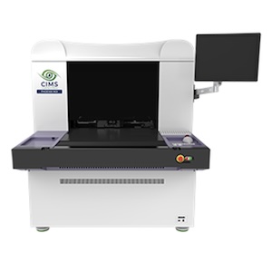
AdvancedPCB has expanded its high-density interconnect (HDI) quality inspection capabilities with the installation of the CIMS Phoenix MDI AOI system in its Chandler, Arizona facility, enabling precision inspection of mechanical drills down to 150 µm in diameter. The investment supports the company’s broader 2026 Technology Acceleration Initiative focused on expanding precision circuit board fabrication capabilities across its U.S. operations.
As drill diameters continue to shrink and layer counts increase, maintaining tight control over hole quality has become essential to yield and reliability. The new AOI machine allows AdvancedPCB to verify fine mechanical drill features earlier in the fabrication process, reducing variability and improving consistency across complex HDI builds.
This added capability elevates AdvancedPCB’s ability to support stacked and staggered microvias and high layer-count designs required in aerospace and defense, AI hardware, and advanced computing applications. By improving early-stage verification, the company can optimize downstream processes such as plating, lamination, and via fill, ultimately increasing overall production stability and repeatability.
“Precision control at every step is what enables reliable HDI manufacturing,” said Greg Halverson, CEO of AdvancedPCB. “As our customers push into tighter geometries and more complex stack-ups, this level of early-stage inspection gives us the process control to deliver consistently, even on the most demanding builds.”
The company's Chandler, Arizona facility plays a key role in supporting advanced, domestic PCB manufacturing. This expanded inspection capability reinforces the company's commitment to delivering high-performance boards with greater process transparency and control.
AdvancedPCB’s 2026 Technology Acceleration Initiative includes coordinated investments across multiple U.S. facilities to expand advanced fabrication technologies, increase capacity, and support next-generation electronic systems.


