-

- News
- Books
Featured Books
- design007 Magazine
Latest Issues
Current Issue
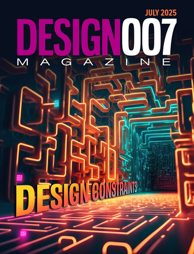
Showing Some Constraint
A strong design constraint strategy carefully balances a wide range of electrical and manufacturing trade-offs. This month, we explore the key requirements, common challenges, and best practices behind building an effective constraint strategy.

All About That Route
Most designers favor manual routing, but today's interactive autorouters may be changing designers' minds by allowing users more direct control. In this issue, our expert contributors discuss a variety of manual and autorouting strategies.

Creating the Ideal Data Package
Why is it so difficult to create the ideal data package? Many of these simple errors can be alleviated by paying attention to detail—and knowing what issues to look out for. So, this month, our experts weigh in on the best practices for creating the ideal design data package for your design.
- Articles
- Columns
- Links
- Media kit
||| MENU - design007 Magazine
OKI Develops 124-Layer PCB Technology for Next-Generation AI Semiconductor Testing Equipment
April 28, 2025 | BUSINESS WIREEstimated reading time: 1 minute
OKI Circuit Technology, the OKI Group printed circuit board (PCB) company, has successfully developed 124-layer PCB technology for wafer inspection equipment designed for next-generation high bandwidth memory, such as HBM mounted on AI semiconductors. This is a roughly 15% increase in the number of layers over conventional 108-layer designs. OTC is seeking to establish mass production technology by October 2025 at its Joetsu Plant in Joetsu City, Niigata Prefecture, which has a proven track record and advanced development and production capabilities in the field of high multilayer, high-precision, large-format PCBs for semiconductor inspection equipment.
AI processing requires the transmission of vast data volumes between graphics processing unit (GPU) semiconductors and memory. As semiconductor performance increases, the memory installed is also required to have high-speed, high-frequency, and high-density data transfer capabilities. HBM features a stacked DRAM structure, requiring technology capable of fabricating wafers even more thinly and precisely. This configuration also requires that the PCBs used in inspection equipment meet even higher levels of performance and quality.
Since the latest semiconductors process an enormous number of signals and the number of wafer-mounted chips increases due to process miniaturization, it is necessary to increase density and more layers on the PCBs used in inspection equipment. Nevertheless, PCB thickness has been limited to 7.6 mm due to various constraints, and 108 layers was the maximum limit with conventional technology. This time, by developing ultra-thin materials and tools and handling technologies suitable for ultra-thin materials, together with developing and introducing a proprietary automatic transport system for ultra-thin materials into its production line, OTC has successfully developed 124-layer PCB technology with a board thickness of 7.6 mm.
OKI is actively engaged in its EMS business based on the core idea of providing comprehensive manufacturing services from design to production and reliability testing. OKI places a particular focus on technology development in the PCB business, and this new technology was developed in response specifically to the areas expected to show future growth, including AI semiconductors, aerospace, defense, robotics, and next-generation communications. OKI will continue to develop PCBs and manufacturing technologies to respond to future progress in technology.
OTC will exhibit at the OTC booth (No.305) at PCB East 2025, which will be held at the Boxboro Regency Hotel and Conference Center in Massachusetts, USA from April 30 to May 2, 2025, to introduce this technology.
Suggested Items
PCBAA Wins Summit Silver Award from the American Society of Association Executives
07/18/2025 | PCBAAPCBAA was one of 38 associations that earned Silver Awards for outstanding contributions for an entry titled: Chips Don’t Float: More Printed Circuit Boards Must be Made in America.
INSPECTIS AB ‘Makes it a Meal’ with Series U50s Advanced Kit
07/18/2025 | INSPECTIS ABFamous chefs the world over maintain that an entrée doesn’t make a great meal without side dishes. At INSPECTIS, we call those ‘sides’ an Advanced Kit.
July 2025 PCB007 Magazine: Sales—From Pitch to PO
07/18/2025 |Though all parts of a company are essential for holistic success, it is a foundational truth that a company lives and dies by its sales. If there are no sales, the company eventually ceases to exist, or as Henry Ford says, “Nothing happens until someone sells something.” In the July issue of PCB007 Magazine, we break down the sales stack and provide a guide to up your sales game.
Silicon Mountain Contract Services Enhances SMT Capabilities with New HELLER Reflow Oven
07/17/2025 | Silicon Mountain Contract ServicesSilicon Mountain Contract Services, a leading provider of custom electronics manufacturing solutions, is proud to announce a significant upgrade to its SMT production capability with the addition of a HELLER 2043 MK5 10‑zone reflow oven to its Nampa facility.
KONIG Launches KP400: Advanced 3D Digital Conformal Coating System for High-Density Electronics
07/15/2025 | KONIGKONIG, a leader in electronic packaging protection solutions, is proud to announce the launch of the KP400 3D Digital Packaging Solution—a breakthrough conformal coating system that brings new levels of precision, speed, and material efficiency to electronics manufacturing.


