-

-
News
News Highlights
- Books
Featured Books
- design007 Magazine
Latest Issues
Current Issue
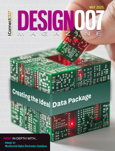
Creating the Ideal Data Package
Why is it so difficult to create the ideal data package? Many of these simple errors can be alleviated by paying attention to detail—and knowing what issues to look out for. So, this month, our experts weigh in on the best practices for creating the ideal design data package for your design.

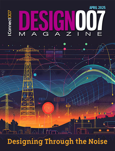
Designing Through the Noise
Our experts discuss the constantly evolving world of RF design, including the many tradeoffs, material considerations, and design tips and techniques that designers and design engineers need to know to succeed in this high-frequency realm.

Learning to Speak ‘Fab’
Our expert contributors clear up many of the miscommunication problems between PCB designers and their fab and assembly stakeholders. As you will see, a little extra planning early in the design cycle can go a long way toward maintaining open lines of communication with the fab and assembly folks.
- Articles
- Columns
Search Console
- Links
- Media kit
||| MENU - design007 Magazine
Siemens, CELUS Collaborate to Empower SMBs with AI-powered PCB Design
October 30, 2024 | SiemensEstimated reading time: 2 minutes
Siemens Digital Industries Software, a global leader in PCB electronic systems design, and CELUS, a pioneer in AI-powered electronic design automation solutions, announced their collaboration to transform the PCB design landscape for small and medium-sized businesses (SMBs) and independent engineers.
This collaboration combines Siemens’ industry-leading PCB design expertise with CELUS' innovative AI automation platform to create a powerful, user-friendly and cost-effective solution tailored to the real-world needs of engineers. The integration of CELUS’ AI-driven automation with Siemens’ next-generation PCB design solution aims to deliver a fully integrated design environment that accelerates design processes, minimizes errors and brings innovative products to market faster and more efficiently.
Empowering engineers with advanced, accessible tools
Engineers and SMBs often face challenges such as tight budgets, limited resources, and the need to juggle multiple roles. Siemens EDA and the CELUS Design Platform are jointly addressing these pain points by simplifying complex PCB design tasks and reducing the time spent on repetitive processes through intelligent automation.
“At Siemens EDA, our mission is to enable innovation and make advanced design tools accessible to businesses of all sizes,” said AJ Incorvaia, senior vice president, Electronic Board Systems, Siemens Digital Industries Software. “Collaborating with CELUS allows us to combine our proven PCB design solutions with front-end, cutting-edge AI automation, providing engineers with the tools they need to innovate efficiently and compete effectively in today's fast-paced market."
Streamlining PCB design with AI automation
CELUS' AI-powered platform automates routine design tasks, such as schematic generation and component selection, allowing engineers to focus on creativity and complex problem-solving. The integration with Siemens’ EDA tools ensures a seamless and flexible design experience, offering a new AI-powered block-level design interface.
"We are extremely excited to work with Siemens to bring our AI-driven automation to a wider audience," said Tobias Pohl, CEO of CELUS. "This collaboration is about empowering engineers by simplifying their workflows, reducing errors and making advanced PCB design more accessible. Together, we're leveling the playing field for SMBs and independent engineers."
Stay informed and visit Siemens at Electronica 2024
Engineers and businesses interested in learning more about the Siemens and CELUS collaboration and future solutions are invited to visit Siemens during Electronica 2024 in Munich from November 12-15, 2024. Engineers are invited to visit the Siemens EDA booth, Hall A3, Booth 561, where CELUS will host demo stations and deliver theatre presentations detailing how AI-driven automation can transform the PCB design process.
Suggested Items
CE3S Launches EcoClaim Solutions to Simplify Recycling and Promote Sustainable Manufacturing
05/29/2025 | CE3SCumberland Electronics Strategic Supply Solutions (CE3S), your strategic sourcing, professional solutions and distribution partner, is proud to announce the official launch of EcoClaim™ Solutions, a comprehensive recycling program designed to make responsible disposal of materials easier, more efficient, and more accessible for manufacturers.
WellPCB, OurPCB Launch Low-Cost PCB Assembly and Custom Cable Assembly Solutions
05/29/2025 | ACCESSWIREWellPCB and OurPCB, world leading PCB manufacturing service providers, announced today that they have officially launched new Low-Cost PCB Assembly Solutions and Custom Cable Assembly services to meet the needs of the electronics manufacturing industry for high cost performance and flexible customization.
Siemens Expands OSAT Alliance Membership to Build Domestic Semiconductor Supply Chains
05/29/2025 | SiemensSiemens Digital Industries Software announced the latest members to join its OSAT Alliance program which enables outsourced semiconductor assembly and test (OSAT) providers to develop, validate and support integrated circuit (IC) package assembly design kits (ADKs) that drive broader adoption of emerging technologies by fabless semiconductor and systems companies and help to build secure domestic semiconductor supply chains.
Standards: The Roadmap for Your Ideal Data Package
05/29/2025 | Andy Shaughnessy, Design007 MagazineIn this interview, IPC design instructor Kris Moyer explains how standards can help you ensure that your data package has all the information your fabricator and assembler need to build your board the way you designed it, allowing them to use their expertise. As Kris says, even with IPC standards, there’s still an art to conveying the right information in your documentation.
High-frequency EMC Noise in DC Circuits
05/29/2025 | Karen Burnham, EMC UnitedEMC isn’t black magic, but it’s easy to understand why it seems that way. When looking at a schematic like that in Figure 1, it looks like you’re only dealing with DC signals all across the board. There’s a 28 VDC input that goes through an EMI filter, then gets converted to 12 VDC power. Except in extremely rare circumstances involving equipment sensitive to magnetostatic fields, DC electricity will never be part of an EMC problem.


