-

- News
- Books
Featured Books
- design007 Magazine
Latest Issues
Current Issue
Rules of Thumb
This month, we delve into rules of thumb—which ones work, which ones should be avoided. Rules of thumb are everywhere, but there may be hundreds of rules of thumb for PCB design. How do we separate the wheat from the chaff, so to speak?

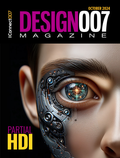
Partial HDI
Our expert contributors provide a complete, detailed view of partial HDI this month. Most experienced PCB designers can start using this approach right away, but you need to know these tips, tricks and techniques first.

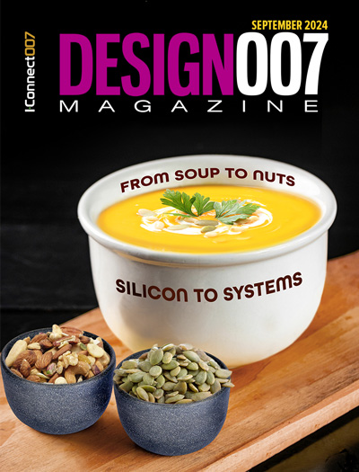
Silicon to Systems: From Soup to Nuts
This month, we asked our expert contributors to weigh in on silicon to systems—what it means to PCB designers and design engineers, EDA companies, and the rest of the PCB supply chain... from soup to nuts.
- Articles
- Columns
Search Console
- Links
- Media kit
||| MENU - design007 Magazine
Highlights of the ICT 50th Anniversary Symposium
October 24, 2024 | Pete Starkey, I-Connect007Estimated reading time: 16 minutes
Why does it always rain when I attend these events? Temperatures were dropping, daylight was shrinking, and there were seasonal colour changes in wet hedgerows as I travelled to Gloucestershire for the 50th Anniversary Symposium of the Institute of Circuit Technology at Puckrup Hall near Tewkesbury in mid-October.
It was a memorable occasion: Nostalgic for my contemporaries who remembered our industry at its most prosperous, technically outstanding in the quality and significance of presentations to an attentive audience of printed circuit professionals, and complemented by the sharing of ideas, information, and trade gossip within a friendly community at the evening gathering.
Delegates were welcomed to the symposium by ICT Technical Director Emma Hudson. She introduced keynote speaker Professor Martin Goosey who gave his personal overview of the past 50 years, entitled “Half a Century of Electronics Innovation,” keeping the audience engrossed and enlightened in his characteristically calm professorial style as he evoked an abundance of memories and reminiscences.
Remarking that much had changed but much remained familiar in a world that had moved from almost no electronics to electronics in everything, he reminded us of some notable earlier dates: Paul Eisler originating the printed circuit in 1938, Bell Labs demonstrating the germanium transistor in 1947 and the silicon transistor in 1954, the development of compound semiconductors such as gallium arsenide in the 1960s, and how transistors in small discrete packages drove the rapid development of the PCB. And the observations and projections made in 1965 by Gordon Moore continue to hold true.
Looking at some macro-level changes over these past 50 years, Professor Goosey used some examples. The motor car transitioned from mechanical, through electro-mechanical to electronics-in-everything. Mobile phones shrunk to their minimum size in the mid-2000s before the introduction of the smartphone, and are now getting larger again. Consumer electronics, home entertainment, and music reproduction equipment has either undergone radical change or been abandoned along the way, and televisions are becoming enormous.
During the 1970s, the UK PCB industry was primarily focused on meeting the needs of a growing electronics sector, with demand driven by the rise of consumer electronics, telecommunications, and military applications. There were variously reported to be between 200 and 400 companies, mainly small-to-medium enterprises, engaged in relatively simple manufacturing of low-cost high-volume product. Dry film photoresist was widely used for imaging. Trends in electronics included colour TVs, transistor radios, electronic calculators, and the first personal computers. The increasing use of integrated circuits was driving the need for more complex PCBs.
Technological advancements during the 1980s included the introduction of more-sophisticated manufacturing techniques, computer-aided design, and automated manufacturing processes. As integration increased and device packages became smaller, circuit designs became more complex and multilayers were progressively more popular. The UK industry began to specialise in certain niche markets, including automotive and aerospace as the demand for high-reliability products grew, and surface mount assembly technology was becoming increasingly popular. There were still reckoned to be between 250 and 300 PCB companies in the UK by the mid-1980s.
The 1990s saw the launch of the World Wide Web in 1991, followed by rapid expansion of the Internet mid-decade and culminating in the dot-com bubble. As the 1990s progressed, the UK PCB industry was significantly impacted by globalisation as competition from low-cost manufacturers in Asia led to consolidation, with many UK companies either merging or outsourcing production to maintain profitability, although there were still between 150 and 200 PCB companies by the end of the decade. The emphasis continued to shift toward high-tech applications, driving innovation in materials and processes, and most high-tech printed circuit boards were using surface mount devices by the late 1990s.
During the 2000s there was a growing awareness of the environmental impact of the electronics industry. The WEEE and RoHS directives drove the introduction of lead-free soldering and banned certain brominated flame retardants. UK PCB manufacturers tended to focus on high-value specialised PCBs for medical, military and aerospace applications, where quality and reliability were critical. Capital investment was typically directed at capability enhancement, particularly in high density interconnection technology. Toward the end of the decade, the number of PCB companies in the UK had continued to decline, with between 40 and 60 remaining in 2010.
Since 2010, the PCB industry had undergone a significant digital transformation, with the adoption of Industry 4.0 concepts including automation, IoT integration and data analytics all impacting manufacturing processes. Sustainability had also become a major focus, with an increasing emphasis on eco-friendly materials and processing. The UK PCB industry, which now numbered around 40, started to promote itself as a leader in sustainable practices in order to appeal to environmentally-conscious clients.
“So, what’s coming next in electronics?” Professor Goosey asked. He believes that the massive leap in computing power offered by quantum computing will revolutionise drug discovery and optimisation, finance, and artificial intelligence by solving complex problems much faster. The integration of AI-specific hardware into devices will enable more efficient and powerful machine learning.
6G wireless technology, with ultra-fast communication speeds and ultra-low latency, will be an enabler for autonomous vehicles, smart cities, and IoT ecosystems. Solid-state batteries offer better energy density, safety, and charging speeds than lithium-ion batteries and are fundamental to the future of electric vehicles. Also on his list were body implants, wearable electronics. and the greater use of robots.
Considering future challenges and opportunities, he sees net-zero/global warming as a leading contender, with renewables, power management, control, and energy storage constituting major roles for AI and 6G.
The increasing use of artificial intelligence offers the prospect of computers or computer-controlled robots to perform tasks associated with humans to reason, discover meaning, generalise, or learn from experience. Whether AI would be a net creator or eliminator of jobs remained to be seen, but the pace of change is quickening.
Professor Goosey closed his presentation by commenting that the transition over the past 50 years from “almost no electronics” to “electronics in everything” has been made possible by increased miniaturisation of semiconductors and greater integration and would be further enabled by development of advanced interconnection and packaging solutions. The next 50 years promises to be just as exciting, if not more so, than the last 50 years.
He quoted Einstein: “I never think of the future—it comes soon enough.”
The Future of PCB Materials
Next to speak was Alun Morgan, president of EIPC, whose subject was “PCB materials: How did we get here and where are we going?” He began by recounting his personal history with the Institute of Circuit Technology, from his original application for membership in June 1981 and his first presentation as a lecturer at ICT’s Preliminary Course on Printed Circuits at Rewley House in Oxford. (A course that had already introduced myself and many of my contemporaries to the basics of PCB manufacturing, all presented via flip charts and slide projectors: no PowerPoint in those days!)
Morgan showed two pages from Circuit World, the Institute’s journal at that time. One included classified adverts from laminate manufacturers—familiar names of the past, like Perstorp, Bakelite, Ferrozell, MAS, Micaply, Norplex, Permali—none of which exist anymore although some have been incorporated into groups such as Isola.
The other page was an editorial by Reg Shemilt, which gave some interesting statistics: “478: that is the latest figure for established printed circuit manufacturers in the UK, with an estimated workforce of some 16,000. Again, from an output of about £30 million in 1975, by 1982 this has increased to over £100 million excluding ‘in-house’ facilities, which it is estimated would double this figure.”
Morgan gave an up-to-date figure for the number of PCB manufacturers in Europe: “169, with a total turnover around 2 billion euro: fewer companies and in general much bigger companies.”
Having established his points of reference, he described how the industry progressed through the intervening years from a substrate material perspective, beginning with a basic definition: “An insulating material, usually a composite comprising a resin and a reinforcement, with a conductor bonded to one or both sides”, and then discussing resins, reinforcements, conductors, and flame retardants in technical and practical detail. He covered his complex topic systematically and comprehensively with clear explanations and meaningful illustrations without losing the attention of his audience. Even those acknowledged as industry experts benefited from the knowledge he shared, particularly regarding recent developments and the current state-of-the-art in laminate technology.
With all the elegant improvements in laminate characteristics and properties over the period, what about laminate prices? Morgan’s example was “standard” FR-4 laminate—considered a speciality in the 1970s but now a basic commodity—costing effectively a third of what it was: the euro equivalent of €50-60 per square metre in 1970 to €20-22 in 2024. “So where do we go from here, now that we are reaching the limits of glass fibre thickness and copper foil profile?” Morgan asked.
First, he looked at markets and applications. Prismark’s figures showed trends in the mix of materials: standard FR-4 trending down while the share of speciality and other laminates grew significantly in a world market whose total value declined from $19 billion in 2021 to $13 billion in 2023.
Although the market value for PCBs is forecasted to grow steadily toward $128 billion in 2030, global semiconductor revenue is expected to grow exponentially to $1.2 trillion during the same period, with 103 new fabs planned worldwide in the next three years, of which 74 are in Asia, 18 in the Americas, and 11 in Europe and Middle East. Morgan’s comment was that although Europe will never catch-up with the volume of investment happening in Asia, the key is to understand where we could benefit. He reiterated comments from his earlier presentations about the fundamental requirement to package the semiconductor chips. Indeed, one of his closing slides showed the enormous range of established and emerging packaging architectures and their substrates.
Nakahara’s list of the world’s top PCB makers indicate that the majority of the leaders make IC substrates, some representing as much as 100% of their revenue, and that substrates accounted for 18.6% of the total worldwide PCB output of about $97 billion in 2022.
Massive investment had been made in the production of IC substrates, which Morgan defined as the interface between the nano-world of the semiconductor and the micro-world of the PCB. There were only three significant manufacturers in Europe, all using Ajinomoto build-up film (ABF). Worldwide, a massive industry has sprung up, principally in Asia. “We’ve got to find our place in all this,” he said. “We’ve got to find what works in Europe and North America because we can’t fight against the volume. We’ve got to find something special. This investment in IC substrates, we’ve got to take it on board, learn how to use materials like ABF, use technologies like embedding and substrate-like PCB, and accept the blurring of the boundaries between the micro-world and the nano-world. Can we get involved in it, either directly or through partnership?”
Circularity in Electronics
With the mission to tackle electronic waste using naturally-derived PCB materials, Jack Herring, inventor of Soluboard and founder of Jiva Materials, described an alternative end-of-life solution for PCBs.
“Mainstream PCB substrates are not designed with recyclability in mind,” he observed as he reviewed the statistics for e-waste, predicted to increase to 82 million tonnes annually by 2030, with printed circuit boards currently representing over 40% and resulting in 6 million tonnes of CO2 emissions annually from existing disposal and recycling processes.
The solution he offered is the world’s first naturally-derived PCB laminate, produced using fully biodegradable and non-toxic natural fibres, which is fully recyclable using a process based on hot water.
Herring was quick to stress that Soluboard is not the universal substrate; designers and OEMs need to consider specific material attributes when creating a new product, and many applications demand particular properties and performance characteristics. But there are certain applications where an alternative could be considered: single use products with shorter lifespans, products recovered via regulatory take-back schemes, reduced CO2 and ESG-driven products as examples. Jiva is developing market opportunities in these areas.
Significant progress was made in 2024 and Herring listed some milestones: plated through-hole capability has been demonstrated; patents have been granted in the UK, US, India, Japan, Korea, Singapore and Taiwan; and a knowledge transfer partnership has been secured with the University of Portsmouth, as well as the appointment of experts in product strategy and business development.
By the end of 2024, Jiva expects to have secured orders from more than 25 customers and to have achieved UL94 V0 flame-only accreditation and ISO 9001:2015 certification. Herring reviewed customer feedback from pilot trials using Soluboard prototypes in various applications to demonstrate the technology in relevant environments.
Page 1 of 2
Suggested Items
IPC Hall of Fame Spotlight Series: Highlighting Patty Goldman
11/22/2024 | Dan Feinberg, I-Connect007In my first article of this special series, I wrote a synopsis of the IPC Raymond E. Pritchard Hall of Fame (HOF) Award, along with a commentary on its first few members, particularly Pritchard. Over the years, IPC members who have contributed significantly to IPC and our industry have been awarded this high honor and recognition. Though many early HOF members have passed away and are unknown to today’s IPC membership, their contributions still resonate. Over the coming months, I look forward to researching and reporting on IPC Hall of Fame members and their contributions. This month, I highlight Patty Goldman.
Meet Polar's New Product Specialist Jess Hollenbaugh
11/21/2024 | Andy Shaughnessy, I-Connect007At PCB West, I spoke with Jess Hollenbaugh, a recent college graduate who has now joined Polar Instruments. In this interview, she shares her journey from a physics student focused on high-energy astrophysics to her new role at Polar. Her insights provide a glimpse into the dynamic opportunities awaiting those who venture into this evolving industry.
Designing for Cost to Manufacture
11/21/2024 | Marcy LaRont, I-Connect007ICAPE's Richard Koensgen, a seasoned field application engineer with a rich background in PCB technology, shares his journey of working with customers and manufacturers through the intricacies of circuit board development and emphasizes the importance of early-stage collaboration with PCB designers. With a focus on tackling the most challenging aspects of PCB design and manufacturing, he discusses everything from layout considerations to the thermal challenges of today's technology when it comes to designing for cost.
Nano Dimension Posts Revenue of Revenue $14.9M in Q3 2024; Up 22% YoY
11/20/2024 | Nano DimensionNano Dimension Ltd., a leading supplier of Additively Manufactured Electronics (AME) and multi-dimensional polymer, metal & ceramic Additive Manufacturing (AM) 3D printing solutions, today announced financial results for the third quarter ended September 30th , 2024 and shared a letter from Yoav Stern, the Company’s Chief Executive Officer and member of the Board of Directors.
Eltek Reports Q3 2024 Financial Results
11/20/2024 | PRNewswireEltek Ltd., a global manufacturer and supplier of technologically advanced solutions in the field of printed circuit boards (PCBs), today announced its financial results for the quarter ended September 30, 2024.


