


 The Shaughnessy Report: Watt About Power Integrity?
 Global PCB Connections: Understanding Your Fabricator’s Capabilities (or Niche)
 Elementary Mr. Watson: Chasing Checkmarks, Not Signal Integrity


Keysight Unveils 3kV High Voltage Wafer Test System for Power Semiconductors
October 10, 2024 | BUSINESS WIREEstimated reading time: 1 minute
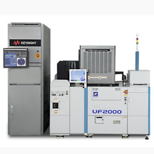
Keysight Technologies, Inc. introduces a 4881HV High Voltage Wafer Test System expanding its semiconductor test portfolio. The solution improves the productivity of power semiconductor manufacturers by enabling parametric tests up to 3kV supporting high and low-voltage in one-pass test.
Manufacturers have traditionally measured wafers using separate testers for high and low voltages. However, demand for power semiconductors is rapidly growing due to their multifunctionality, higher performance, and next-generation devices such as silicon carbide (SiC) and gallium nitride (GaN). As a result, customers need a solution to more accurately and efficiently test their devices and reduce time to market.
Keysight’s solution addresses these challenges by allowing power device makers to perform process control monitoring (PCM) and wafer acceptance testing (WAT) in manufacturing. The new test system delivers the following benefits:
High-Voltage Capability to Meet Future Needs: The high-voltage switching matrix (HV-SWM) supports up to 3kV requirements, is scalable up to 29 pins, and integrates with precision source measure units (SMUs). It enables highly flexible measurements from low current down to sub-pA resolution up to 3kV at any pins. Additionally, high-voltage capacitance measurement and various parametric tests are supported.
One-pass Testing Increases Productivity and Efficiency: The HV-SWM enables a single test system instead of separate high-voltage and low-voltage test systems. Utilizing one system is more efficient and reduces the required footprint and testing time. The system integrates with factory automation environments using Keysight’s SPECS-FA software, which improves the efficiency of the entire production process.
Enhanced Safety and Reliability: The test system has built-in protection circuitry and machine control, ensuring operators and equipment are not impacted by high-voltage surges during a test, and is compliant with safety regulations, including SEMI S2 standards.
Shinji Terasawa, Vice President and General Manager of Keysight's Wafer Test Solutions, said: “Keysight is thrilled to introduce our new wafer test system for power semiconductors, building on our long tenure of testing advanced semiconductors. Our mission is to lead the market by providing cutting-edge solutions that anticipate and meet the rapidly evolving needs of the semiconductor sector. This latest innovation exemplifies our unwavering commitment to the industry.”
Share on:


Testimonial
"We’re proud to call I-Connect007 a trusted partner. Their innovative approach and industry insight made our podcast collaboration a success by connecting us with the right audience and delivering real results."
Julia McCaffrey - NCAB GroupSuggested Items
Datest Marches Into SMTA International with Backup Plans, Big Partnerships, and Bigger X-rays
10/06/2025 | DatestDatest, the industry’s favorite second set of eyes (and hands, and solder joints), is heading to SMTA International 2025 at the Donald E. Stephens Convention Center in Rosemont, IL. Find us at Booth #2627, where high-reliability, high-complexity builds meet their match.
Discover TRI's AI Ecosystem at productronica 2025
09/25/2025 | TRITest Research, Inc. (TRI), the leading test and inspection systems provider for the electronics manufacturing industry, is excited to announce its participation at productronica 2025, which will be held at Messe München Center from November 18 to 21, 2025.
TTCI Wins 2025 Mexico Technology Award for Test Services
09/22/2025 | TTCIThe Test Connection Inc. (TTCI), a trusted provider of electronic test and manufacturing solutions for more than 45 years, is honored to receive the 2025 Mexico Technology Award in the Test Services category.
TTCI Returns to SMTAI with Focus on Functional Test, ICT, and Training Excellence
09/22/2025 | TTCIThe Test Connection Inc. (TTCI), a trusted provider of electronic test and manufacturing solutions for more than 45 years, will exhibit in Booth 2403 at SMTA International 2025, taking place October 19–23 at the Donald E. Stephens Convention Center in Rosemont, Illinois. TTCI will spotlight its advanced test capabilities and full-service approach to tackling complex product validation challenges.
TTCI and The Training Connection Strengthen Electronics Manufacturing with Test Services and Training at PCB West 2025
09/16/2025 | The Test Connection Inc.The Test Connection Inc. (TTCI), a trusted provider of electronic test and manufacturing solutions, and The Training Connection LLC (TTC-LLC) will exhibit at PCB West 2025, taking place Wednesday, October 1, 2025, at the Santa Clara Convention Center in California. Visitors are invited to Booth 113 to explore the companies’ complementary expertise in test engineering services and workforce development for the electronics industry.