-

- News
- Books
Featured Books
- design007 Magazine
Latest Issues
Current Issue
Rules of Thumb
This month, we delve into rules of thumb—which ones work, which ones should be avoided. Rules of thumb are everywhere, but there may be hundreds of rules of thumb for PCB design. How do we separate the wheat from the chaff, so to speak?

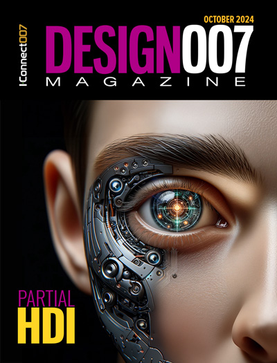
Partial HDI
Our expert contributors provide a complete, detailed view of partial HDI this month. Most experienced PCB designers can start using this approach right away, but you need to know these tips, tricks and techniques first.

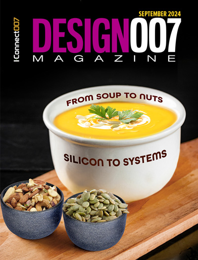
Silicon to Systems: From Soup to Nuts
This month, we asked our expert contributors to weigh in on silicon to systems—what it means to PCB designers and design engineers, EDA companies, and the rest of the PCB supply chain... from soup to nuts.
- Articles
- Columns
Search Console
- Links
- Media kit
||| MENU - design007 Magazine
Cross-domain Design: The Key to Managing Complex Methodologies
September 23, 2024 | Andy Shaughnessy, Design007 MagazineEstimated reading time: 1 minute
For years, Cadence Design Systems has been developing EDA tools that enable the design of ICs and PCBs. Now, as systems continually become more complex, the lines are blurring between these disciplines, and EDA companies are providing designers of PCBs and ICs the ability to understand what’s happening upstream and downstream.
We asked John Park, product management group director for advanced IC packaging at Cadence, to discuss this ongoing convergence of domains, as well as what it all means to designers and design engineers.
Andy Shaughnessy: We’re seeing more technologists pointing out the need for PCB designers to focus on silicon-to-systems. What does that term mean to an EDA company like Cadence?
John Park: We would call this cross-domain co-design. Dealing with the complexity and costs of electronic systems, the over-the-wall approach to design leads to project delays and higher costs. It’s critical that IC designers collaborate with the packaging team and the PCB layout teams to create a fully optimized system at a lower cost. PCB layout designers are now influencing the package pinouts of large BGA/LGA packages. This can lead to better system-level signal quality, better power delivery, and fewer layers required to achieve these performance objectives. This can be especially true for very complex PCB form factors. This means two things: 1) Providing our customers with a common system collaboration and optimization tool across the IC design, package design, and PCB layout; 2) Seamless data exchange between the design tools, including seamless integration from layout to analysis and signoff.
Shaughnessy: What are the most important things that PCB designers need to understand about silicon and packages?
Park: The current trend, driven by size limitations and cost, is to disaggregate huge monolithic ICs into smaller building blocks called chiplets. This shifts much of the complexity from IC design to package design. At the same time, the IC foundries have entered the advanced packaging space with technologies that facilitate higher interconnect density and smaller pin pitches. The industry calls this “multi-chiplet heterogeneous integration” because the individual chiplets can be built from multiple nodes and technologies. As a result, more emphasis is put on multi-chiplet packaging as the platform to create product differentiation.
To read this entire conversation, which appeared in the September 2024 issue of Design007 Magazine, click here.
Suggested Items
Rules of Thumb for PCB Layout
11/21/2024 | Andy Shaughnessy, I-Connect007The dictionary defines a “rule of thumb” as “a broadly accurate guide or principle, based on experience or practice rather than theory.” Rules of thumb are often the foundation of a PCB designer’s thought process when tackling a layout. Ultimately, a product spec or design guideline will provide the detailed design guidance, but rules of thumb can help to provide the general guidance that will help to streamline the layout process and avoid design or manufacturing issues.
PCB Design Software Market Expected to Hit $9.2B by 2031
11/21/2024 | openPRThis report provides an overview of the PCB design software market, detailing key market drivers, challenges, technological advancements, regional dynamics, and future trends. With a projected compound annual growth rate (CAGR) of 13.4% from 2024 to 2031, the market is expected to grow from USD 3.9 billion in 2024 to USD 9.2 billion by 2031.
KYZEN to Spotlight KYZEN E5631, AQUANOX A4618 and Process Control at SMTA Silicon Valley Expo and Tech Forum
11/21/2024 | KYZEN'KYZEN, the global leader in innovative environmentally friendly cleaning chemistries, will exhibit at the SMTA Silicon Valley Expo & Tech Forum on Thursday, December 5, 2024 at the Fremont Marriott Silicon Valley in Fremont, CA.
Flexible Thinking: Rules of Thumb: A Word to the Wise
11/20/2024 | Joe Fjelstad -- Column: Flexible ThinkingIn the early days of electronics manufacturing—especially with PCBs—there were no rules. Engineers, scientists, and technicians largely felt their way around in the dark, making things up as they went along. There was a great deal of innovation, guessing, and testing to make sure that early guidelines and estimates were correct by testing them. Still, they frequently made mistakes.
Cadence Unveils Arm-Based System Chiplet
11/20/2024 | Cadence Design SystemsCadence has announced a groundbreaking achievement with the development and successful tapeout of its first Arm-based system chiplet. This innovation marks a pivotal advancement in chiplet technology, showcasing Cadence's commitment to driving industry-leading solutions through its chiplet architecture and framework.


