


 Fresh PCB Concepts: Engineering Copper Coin and Copper Pedestal Technology With IPC Design Interpretation
 Target Condition: Signal Integrity Without Borders
 Elementary, Mr. Watson: PCB Education in the Midst of the Storms


The use of potassium bromide in the production of graphene on a copper surface can lead to better results. When potassium bromide molecules arrange themselves between graphene and copper, it results in electronic decoupling. This alters the electrical properties of the graphene produced, bringing them closer to pure graphene, as reported by physicists from the universities of Basel, Modena and Munich in the journal ACS Nano.
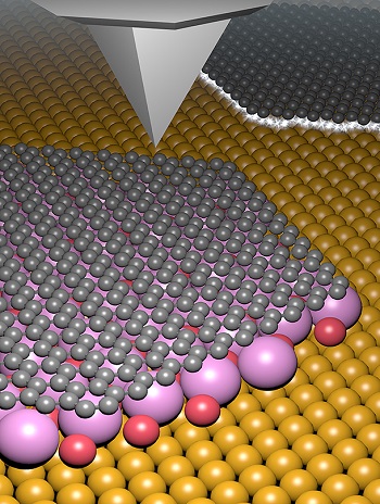
Image Caption: Potassium bromide molecules (pink) arrange themselves between the copper substrate (yellow) and the graphene layer (gray). This brings about electrical decoupling, as demonstrated by scanning probe microscopy studies.
Graphene consists of a layer of carbon atoms just one atom in thickness in a honeycomb pattern and is the subject of intensive worldwide research. Thanks to its high level of flexibility, combined with excellent stability and electrical conductivity, graphene has numerous promising applications—particularly in electronic components.
Molecules for Decoupling
Graphene is often produced via a chemical reaction on metallic surfaces in a process known as chemical vapor deposition. The graphene layer and the underlying metal are then electrically coupled, which diminishes some of the special electrical properties of graphene. For use in electronics, the graphene has to be transferred onto insulating substrates in a multistep process, during which there is a risk of damage and contamination.
In order to obtain defect-free, pure graphene, it is therefore preferable to decouple the graphene electrically from the metallic substrate and to develop a method that allows easier transfer without damage. The group led by Professor Ernst Meyer from the Department of Physics and the Swiss Nanoscience Institute (SNI) of the University of Basel is investigating ways of incorporating molecules between the graphene layer and the substrate after the chemical deposition process, which leads to this type of decoupling.
Altering Electrical Properties
In a study carried out by SNI doctoral student Mathias Schulzendorf, scientists have shown that potassium bromide is ideally suited to this. Potassium bromide is a soluble hydrogen bromide salt. Unlike the chemically similar compound sodium chloride, potassium bromide molecules arrange themselves between the graphene layer and the copper substrate. This was demonstrated by researchers in a variety of scanning probe microscopy studies.
Calculations performed by colleagues at the University of Modena and Reggio Emilia (Italy) explain this phenomenon: It is more energetically advantageous for the system if potassium bromide molecules arrange themselves between the graphene and copper than if they are deposited on the graphene—as happens with sodium chloride.
The researchers have shown that the intermediate layer of potassium bromide alters the electrical properties of graphene—until they correspond to those expected for free graphene. “Our work has demonstrated that the graphene and the underlying metal can be decoupled using potassium bromide, bringing us a key step closer to producing clean and defect-free graphene,” says project supervisor Dr. Thilo Glatzel, who is a member of Meyer’s team.


