









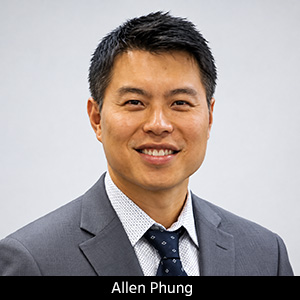






At SEMICON West, I caught up with Allen Phung, head of sales at Koh Young America, where we pivoted from our more traditional focus on SMT-related tech to talking about semiconductors and advanced packaging. Koh Young’s semiconductor business provides inspection and metrology systems for advanced packaging, including micro-solder deposits, high-density substrates, and wafer-level packaging, addressing the demanding requirements as components shrink and interconnect complexity grows.
Marcy LaRont: Advanced packaging is a big deal for the industry, where inspection challenges, an area where Koh Young excels, are becoming even more challenging. What inspection challenges are your customers finding the hardest to solve right now, and how have these helped shape Koh Young's development priorities?
Allen Phung: As you know, we've done very well in the SMT market, and as we expand into the chip scale packaging market, we understand that this application presents new inspection challenges on both the SMT and semiconductor sides of manufacturing. We have developed two newer solutions that address specific issues: Meister S+ and Meister D+. That’s what we are focused on at SEMICON West.
LaRont: When it comes to inspection on SMT vs. semiconductor, is it really just an issue of scale, or is it a whole different ball game?
Phung: It's a couple of things. There is the issue of scale—everything becomes smaller and denser with semiconductors—but you also encounter different applications. You get a much tighter pitch on the component side, and you may be working with different materials on the interface side, whether it's flux, micro paste deposits, or even bumps.
LaRont: What bump size are we talking about these days?
Phung: It’s a range. Some applications still use relatively large bumps; others are going very small, down to a 10-micrometer bump height and a 100-micrometer diameter.
LaRont: What is the Meister S+ designed to do?
Phung: There are two things we see prevalently in this market when it comes to inspection. First, we’ve noticed that many people are now using solder flux as an interface material instead of just solder paste, and that obtaining accurate flux measurements presents a new set of metrology challenges. That drove us to create the Meister S+, which is designed specifically for flux inspection.
It’s our SPI version for the chip-scale packaging application. Flux looks very different from solder paste. It's basically transparent and commonly used for smaller paste deposits. We've put a lot of work into developing our own AI solution, identifying and measuring flux, and then automating that measurement.
LaRont: What is Meister D+?
Phung: The other thing we have observed in this market happens further downstream. Accurate component inspection has become more challenging, which drove the creation of Meister D+. In chip scale packaging, there are a lot of reflective features that must be inspected, especially the back sides of dies. Meister D+ is particularly adept at inspecting highly-reflective features.
In chip-scale packaging, it's the equivalent of AOI for SMT, in that they’re both looking at components. In semiconductor applications, you get much smaller components and tighter pitch. Measuring components with pitches down to maybe 20 microns is challenging. Meister D+ excels here because of its very high resolution.
When you're measuring the size of a component, you must also accurately identify the immediate surrounding area, which is another inspection challenge. That's where gap or pitch between components becomes important.
LaRont: Is that where having reflective surfaces could be a problem?
Phung: Yes, moiré has always had difficulty with highly reflective surfaces. In response to that, we have developed new lighting that makes surface mapping easier, enabling accurate handling, measurement, and inspection.
When you are measuring a component, you are also measuring the surface around that component. The Meister D+ is doing a full 3D topography of that feature. So, we can tell you the actual dimensions of that feature, the length, width, thickness, any warpage, or tilt that has happened. This capability also allows the Meister D+ to inspect dies recessed within a cavity, measuring the die’s surface profile to measure height, tilt, and warpage.
LaRont: Is it primarily the cameras that have changed so much inside of a machine, or did you have to re-engineer it entirely?
Phung: It has been a re-creation of the entire engine: imaging, projection, resolution, and lighting.
LaRont: We talk all the time about how the PCB, SMT, and semiconductor industries are coming closer together through HDI, UHDI, and substrate interconnect technology. What else changes when inspection moves from SMT to wafer-level packaging?
Phung: A lot of the change comes down to the form factor you're handling. As we move upstream in the process away from the packaging, we're handling an entire wafer. That is where ZenStar becomes important because it is specifically designed to measure bumps on the wafer surface. You can imagine a whole different set of challenges because now, the entire surface of this wafer is reflective. We developed ZenStar specifically for that application. We’re dealing with a range of bump sizes, from large to very small, down to 30–40 microns in diameter. The tool must be able to measure accurately over a big range.
LaRont: Is this a new area for Koh Young?
Phung: Yes, wafer inspection is new for Koh Young, and we are seeing strong demand and great success. Our primary focus is on 300 mm wafers.
LaRont: From what I understand, 300 mm is a significant focus for the whole semiconductor industry. Allen, how is Koh Young using AI to help with inspection, detection, and validation?
Phung: I believe AI is where Koh Young really separates us from the competition. We were early adopters, and we are using AI throughout the process, from preparation to analysis. Process preparation leverages our 3D technology, measuring everything, so we can use that information to automatically program the system to inspect and have preset pass-fail tolerances for a particular feature.
On the inspection side, the extensive use of AI technology is completely transparent to the user. Additional engines and filters run in the background on the machine to ensure our measurements are accurate and repeatable. In post-inspection, you have the outcome the system generated. Instead of a heavy reliance on human operators to review the output, an AI agent previews everything and considers additional operator inputs, which dynamically change what the AI agent considers pass or fail. At the end of the day, it greatly improves the first-pass yield of that process.
But we wanted to go one step further beyond the system. We are taking our inspection solutions and delivering value upstream, where our process optimizer software comes into play. Our AI engine analyzes the inspection results and decides what action the upstream equipment should take. We may feed that information into the equipment and have an operator implement those actions, but in some instances, our inspection system will actually take full control of the upstream process equipment and automatically make the changes.
The benefits are twofold: It improves the process and contributes to process maintenance during the production cycle, which, I think, is where everyone hopes to go with this.
LaRont: Everyone wants more automation, and you've got AI fully on both the front and back ends.
Phung: Yes, and we offer them in incremental pieces, so there's something for everyone, depending on how far a customer wants to take it.
LaRont: Allen, as manufacturers pursue finer pitches, larger packages, and panel-level processing, where do you see the next major inspection bottlenecks?
Phung: I see that bottleneck happening as production volumes scale, whether you are talking about very small or very large products. With the huge boom in AI infrastructure, those products have a very large form factor with a very complex layout, which is why 3D is so important for accurate measurement.
Beyond AI, the space industry is booming. With the prevalence of low-earth orbit satellites, we must ensure reliability in these products, controlling whether something is good or bad before it is sent into space. Reworking completed assemblies is often very difficult, but in space it's almost impossible.
LaRont: Allen, do you have any closing thoughts?
Phung: We are excited about the future. Our technologies will really help customers improve yields, reduce costs, and improve their manufacturing processes.
LaRont: Thank you, Allen. It was great to visit with you.