















 It’s Only Common Sense: When the Cheapest Board Becomes the Most Expensive
 The Chemical Connection: Employee and Operator Empowerment in the Age of AI
 The Big Picture: Not One, But Three Grey Rhinos





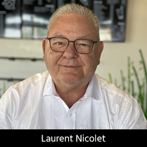
Fabricators are confronting process requirements today that would have seemed foreign to the PCB shop not long ago, presenting both a promise and a significant manufacturing challenge. SCHMID is one company rising to it in big ways. SCHMID's Laurent Nicolet, VP for the Business Unit PCB, talks about the convergence between PCB fabrication and semiconductor processing as feature sizes shrink, the emergence of glass as an attractive substrate and interposer material, and SCHMID’S embedded trace technology and the work toward moving that technology into high-volume manufacturing.
Marcy LaRont: Laurent, tell me about the work SCHMID is doing in advanced manufacturing. What are you working on?
Laurent Nicolet: There are two significant things that are worth talking about. One is our embedded trace process for PCBs, though we are still quite early in the game in terms of industry readiness for adoption.
The other has to do with the tremendous amount of interest we are seeing in redistribution layers (RDL), the microscopic network of fine copper wiring built directly onto a glass substrate or glass core, and photo-imageable polyimide (PID) material for panel leveling, which is easier to proceed through a lithography process than ABF, although it has some material issues compared to ABF.
Our InfinityLine C+ is a vertical rotating wet-processing cluster system designed specifically for high density panel-level packaging (PLP), in that it treats both sides of HDI PCB or substrate simultaneously. We are going close to the submicron level: 0.8-micron vias and 1-micron line-and-space. That is also quite a significant development for the industry right now.
LaRont: What are some of the technical nuances specific to panel-level packaging and working with glass substrates?
Nicolet: When working with these glass-core substrates, you are ultimately looking at a thickness of 0.8 to 1.10 millimeters. Because it is glass, the handling is more delicate. For PLP you have material thicknesses up to 6 millimeters, including carrier systems, and weights up to 4 or 5 kilograms, with warpage up to 4-6 millimeters. Because of these intense physical dimensions, handling the material safely through the machine becomes incredibly critical.
The working environment for PLP is approaching semiconductor-grade levels. These process technologies are beginning to show similarities.
This also means we are now playing in an ISO Class 5 clean environment. The filtration of the solutions, liquid, in use in these tools needs to have filtration down to 0.05 µm. Our machines will be modified to meet ISO Class 5 standards.
We have also created a new product called QuantumLine, a manufacturing equipment platform designed specifically for producing next-generation glass-core substrates for advanced semiconductor packaging. It is built to run in a Class 5 cleanroom and is aimed at manufacturing quantum-level computing.
Continue reading this interview in the September 2026 issue of I-Connect007 Magazine.