













 It’s Only Common Sense: Win the Sale Before the RFQ Arrives
 The Marketing Minute: Marketing Is a Team Sport





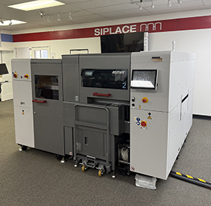
Technica USA, together with the ASMPT team, recently hosted CM and OEM customers for private demonstrations of the SIPLACE CA2 at Technica’s Demo & Applications Center in San Jose. The advanced placement system combines high-speed chip assembly directly from the wafer with conventional SMT placement in a single machine.
Smart devices, 5G communications, and autonomous driving are transforming the way we live and work. Enabling these innovations is the continued miniaturization of electronics, combined with ever-increasing demands for functionality, performance, and system complexity.
At the heart of this evolution is System in Package (SiP) technology, which integrates ICs and SMT components into a compact, highly sophisticated system. By combining multiple functions within a smaller footprint, SiP enables manufacturers to achieve greater functionality and performance while meeting the demands of increasingly complex electronic applications.
The SIPLACE CA2 brings this advanced technology directly to the SMT production line. Combining the capabilities of an SMT placement machine and a die bonder, the system can process both SMDs supplied from changeover tables and feeders and dies taken directly from the sawn wafer, all within a single production step.
By integrating die bonding directly into the SMT production process, the SIPLACE CA2 eliminates the need for dedicated die-bonding equipment, helping manufacturers streamline production while reducing equipment and material-handling requirements. With reduced operator intervention, advanced connectivity, and integrated data utilization, the SIPLACE CA2 is designed to support the requirements of the Intelligent Factory.
Yannick Green, Bay Area Account Manager for Technica USA, stated: “We really appreciated the great turnout we had each day for these private demonstrations. Our customers were thoroughly impressed with the capability and speed of this placement technology. The ability to place dies directly from the wafer eliminates the traditional taping process, reducing material handling while simplifying production. In a 24/7 SiP production environment, direct wafer placement can eliminate the need for up to 800 kilometers of tape per year, helping reduce material consumption, operating costs, and the environmental impact of production.”
For customers who were unable to attend the SIPLACE CA2 Demo Week, Technica USA invites you to contact your local Technica sales representative or email sales@technica.com to learn more about this advanced placement technology and its potential applications.
As a subsidiary of EMC Taiwan, Technica USA continues to expand its market presence by broadening its portfolio of advanced manufacturing technologies across established and emerging markets. Through strategic partnerships with customers and leading technology suppliers, Technica USA remains committed to supporting the electronics manufacturing industry with world-class equipment, technical expertise, applications support, and innovative manufacturing solutions.