









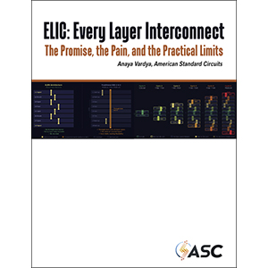








Every layer interconnect (ELIC) is an architectural statement about how a PCB is built, signaling a fundamental shift in how we think about routing density, vertical interconnect, and the relationship between design and fabrication.
To understand what ELIC solves, you have to understand what it replaces. Traditional HDI construction uses a rigid core with sequential build-up layers on one or both sides:configurations such as 2-4-2 or 3-2-3. In those designs, microvias connect only adjacent build-up layers. Through-holes serve the core. The result is a predictable, well-characterized architecture, but one that is fundamentally limited in how tightly you can pack interconnects, because the through-hole barrel consumes real estate from one side of the board to the other regardless of whether the signal needs to traverse every layer.
ELIC eliminates the through-hole as the primary vertical interconnect. In a true every-layer interconnect architecture, each layer connects to the adjacent layer above and below exclusively through laser-drilled microvias. Every layer is a potential routing layer. Pads only occupy the layers where the net actually needs to be. The via stub disappears, and the annular ring footprint shrinks. The result is a board that can support the escape routing demands of the most aggressive sub-100-micron pitch BGAs and advanced packaging formats without sacrificing layers to plumbing that was never needed in the first place.
What’s driving this? Semiconductor packages are shrinking their pitch while increasing I/O count. SoCs, advanced memory stacks, and RF front-end modules are pushing designers into territory where traditional HDI construction cannot provide enough routing channels in the available space. Board thickness envelopes are also tightening in wearables, implantables, and aerospace avionics. Every millimeter of Z-axis matters and ELIC addresses all of these simultaneously.
To continue reading this article, which appeared in the June 2026 edition of I-Connect007 Magazine, click here.