


 It’s Only Common Sense: Build Your Business on Reputation, Not Neglect
 The Marketing Minute: If Your Marketing Budget Gets Cut in Half, Then What?


Absolute EMS, Inc., a six-time award-winning provider of fast turnaround, turnkey contract electronic manufacturing services (EMS), is drawing attention to the critical role of 3D Solder Paste Inspection (SPI) in ensuring the reliability of both FLEX and rigid printed circuit board assemblies (PCBAs).
Industry data shows that nearly 30 percent of PCBA defects stem from poor solder paste application, an issue that can have serious consequences in markets such as medical, defense, and aerospace, where Absolute EMS serves as a manufacturing partner. By incorporating inline 3D SPI across its lines, the company ensures precision in one of the most sensitive stages of PCB assembly.
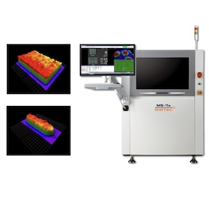
Unlike traditional 2D inspection methods, 3D SPI measures solder paste volume, height, area, and shape on every pad, capturing data in real time and flagging even the smallest deviations. The process also feeds data back to stencil printers, allowing for immediate corrections before defects propagate downstream.
“SPI isn’t an optional step for us — it’s a safeguard built into every board we manufacture,” said Doug Dow, COO at Absolute EMS. “Especially with FLEX assemblies, where paste control is more demanding, SPI gives us the visibility needed to avoid defects and deliver repeatable results.”
The Absolute EMS SPI process follows a series of tightly controlled steps:
- PCB preparation to remove contaminants and ensure optimal surface conditions.
- Solder paste application via stencil printing, where any slight variation can affect final assembly.
- 3D scanning with high-resolution cameras and projectors, measuring paste attributes against defined specifications.
- Analysis and reporting, where results outside set limits trigger alerts and adjustments.
Among the most common issues detected are insufficient or excessive paste volume, solder bridges, misalignment, and irregular paste shapes — all of which can compromise the performance of a finished assembly. By catching these errors early, Absolute EMS reduces rework, shortens cycle times, and strengthens process yields.
3D SPI is part of a broader inspection and quality assurance strategy at Absolute EMS, which also includes inline 3D Automated Optical Inspection (AOI) and 3D X-ray inspection of solder joints. Together, these systems provide a multi-layered view of assembly quality, giving customers confidence in products that often operate in mission-critical environments.
Absolute EMS continues to expand its inspection capabilities in line with growing demand for high-density, high-reliability assemblies, positioning itself as a trusted partner for customers in markets where precision is non-negotiable.


