-
- News
- Books
Featured Books
- pcb007 Magazine
Latest Issues
Current IssueAdvancing the Advanced Materials Discussion
Moore’s Law is no more, and the advanced material solutions to grapple with this reality are surprising, stunning, and perhaps a bit daunting. Buckle up for a dive into advanced materials and a glimpse into the next chapters of electronics manufacturing.
Inventing the Future With SEL
Two years after launching its state-of-the-art PCB facility, SEL shares lessons in vision, execution, and innovation, plus insights from industry icons and technology leaders shaping the future of PCB fabrication.
Sales: From Pitch to PO
From the first cold call to finally receiving that first purchase order, the July PCB007 Magazine breaks down some critical parts of the sales stack. To up your sales game, read on!
- Articles
- Columns
- Links
- Media kit
||| MENU - pcb007 Magazine
IIT Kharagpur, A*STAR Singapore Forge Strategic Partnership to Advance Semiconductor Innovation in Asia
June 3, 2025 | IIT KharagpurEstimated reading time: 1 minute

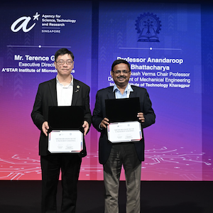
In a landmark move to foster global collaboration in semiconductor research and talent development, IIT Kharagpur has signed a Memorandum of Understanding (MoU) with the Institute of Microelectronics (IME) under Singapore’s Agency for Science, Technology and Research (A*STAR). The announcement was made during SEMICON Southeast Asia 2025, where IIT Kharagpur represented India’s academic and technological prowess in the semiconductor domain.
This partnership underscores the shared commitment of India and Singapore to build a resilient, innovative, and skilled semiconductor ecosystem through international collaboration. IIT Kharagpur, India’s premier institution for science and technology, brings decades of expertise in microelectronics, chip design, nano-fabrication, and advanced materials, making it a key technical partner in this alliance.
As India scales its ambitions in semiconductor manufacturing and R&D, this collaboration positions IIT Kharagpur at the forefront of global initiatives aimed at strengthening semiconductor value chains. The MoU opens new avenues for joint research in Advanced CMOS and post-CMOS technologies; Heterogeneous integration and packaging; AI hardware accelerators; Next-generation memory systems; Photonics and quantum devices; Chip reliability, Thermal Management and Failure Analysis. The collaboration also supports exchange programmes for students and researchers, knowledge-sharing workshops, and co-development of training modules to develop future-ready semiconductor talent.
Prof. Anandaroop Bhattacharya, Dept. of Mechanical Engineering, IIT Kharagpur stated, “This MoU with A*STAR IME marks a significant step in IIT Kharagpur’s global ambition to drive semiconductor innovation. As India rapidly moves to become a semiconductor hub, academia-industry-government collaborations like this will be crucial in building a robust, self-reliant, and globally competitive semiconductor ecosystem.”
Prof. Yeo Yee Chia, Deputy Chief Executive (Innovation & Enterprise) at A*STAR commented, “Singapore's semiconductor ecosystem is built on strong collaborations between public agencies, academia, and industry partners. The Innovate Together event exemplifies our commitment to fostering these partnerships and accelerating innovation to address industry challenges and capture new opportunities in the global semiconductor landscape.”
The signing was part of A*STAR’s broader initiative to connect with international institutions, including partners from Uzbekistan and Singapore’s own semiconductor industry. The Innovate Together event held alongside SEMICON Southeast Asia 2025 highlighted the importance of cross-border collaborations in addressing complex challenges in semiconductor manufacturing, design, and integration.
Testimonial
"Our marketing partnership with I-Connect007 is already delivering. Just a day after our press release went live, we received a direct inquiry about our updated products!"
Rachael Temple - AlltematedSuggested Items
Advanced Semiconductor Packaging Market Sees Rising Adoption Across Automotive and Industrial Sectors
10/14/2025 | openPRThe semiconductor packaging market size is estimated to reach at a CAGR of 7.2% during the forecast period (2024-2031).
SEMICON West: The Path to a $1 Trillion Future
10/14/2025 | Marcy LaRont, I-Connect007After more than 50 years in San Francisco, SEMICON West moved its 2025 show to Phoenix, which is significant because it highlights the importance of Arizona as a semiconductor and tech hub. Though the show will be back in San Francisco in 2026, the overwhelmingly warm welcome SEMI received from Arizona Governor Katie Hobbs, Phoenix Mayor Kate Gallego, and ASU President Michael Crowe—who has been responsible for ASU repeatedly achieving the U.S. News and World Reports most innovative university ranking—was remarked upon repeatedly. All indications are that SEMICON West may well be back in Phoenix after that 2026 season.
Is Glass Finally Coming of Age?
10/13/2025 | Nolan Johnson, I-Connect007Substrates, by definition, form the base of all electronic devices. Whether discussing silicon wafers for semiconductors, glass-and-epoxy materials in printed circuits, or the base of choice for interposers, all these materials function as substrates. While other substrates have come and gone, silicon and FR-4 have remained the de facto standards for the industry.
Thallner Recognized for Leadership and Innovation in Semiconductor Equipment and MEMS Manufacturing
10/10/2025 | SEMISEMI, the industry association serving the global semiconductor and electronics design and manufacturing supply chain, announced Erich Thallner, President and Co-founder of EV Group (EVG), as its first SEMI Americas Catalyst Award recipient at SEMICON West 2025.
I-Connect007 Editor’s Choice: Five Must-Reads for the Week
10/10/2025 | Nolan Johnson, I-Connect007I-Connect007 has a new monthly digest newsletter, the Advanced Electronic Packaging Digest, and as I was scanning our advanced packaging newsfeeds this week, I came across a primer from tokenring.ai (republished through station WRAL, Raleigh, North Carolina), which I found quite useful. Whether you’re a designer, fabricator, or assembler, the package schemes being developed will change how you work, so be sure to keep your eye on the technological horizon and subscribe to the monthly Advanced Electronic Packaging Digest.