


 Dan's Biz Bookshelf: 'Apple in China: The Capture of the World’s Greatest Company'
 The Chemical Connection: Experience and Wisdom Gained by Doing Business
 It's Only Common Sense: Leveraging AI in Your Sales Strategy


Material Selection and RF Design
April 21, 2025 | Andy Shaughnessy, Design007 MagazineEstimated reading time: 1 minute
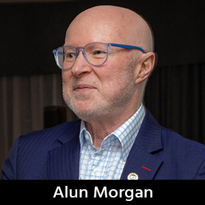
Innovation rarely sleeps in this industry, and the RF laminate segment offers a perfect example. RF materials have continued to evolve, providing PCB designers much more than an either/or choice. I asked materials expert Alun Morgan, technology ambassador for the Ventec International Group, to walk us through the available RF material sets and how smart material selection can ease the burden on RF designers and design engineers.
Andy Shaughnessy: Alun, just give us a quick refresher: How are RF materials different from traditional PCB laminates?
Alun Morgan: RF covers a broad range of frequencies, often defined as the spectrum from 3 KHz to 300 GHz. At the low end, traditional materials are fine; however, the influence of the material becomes much more critical as frequency increases.
Shaughnessy: How does RF differ from HSD (high-speed digital)?
Morgan: They are two different worlds, with very different design requirements. RF is primarily concerned with the propagation of analog waveforms, whereas HSD is primarily concerned with the transmission of binary digital bitstreams. Each has its particular benefits and drawbacks. The good news is that materials designed for high-speed digital applications are also generally suitable for high-frequency analog circuits.
Shaughnessy: What do PCB designers moving into the RF space need to understand about material selection?
Morgan: There are some very specific electrical properties that are important when selecting materials for RF or HSD applications. The first is the dielectric constant (Dk) of the material. The Dk is the ability of the substrate to store electric energy in an electrical field. It is a dimensionless property and is quoted as a value relative to a vacuum, which has a Dk of 1. Why does it matter? It matters because it determines transmission speed and must be accounted for when calculating the timing and synchronization of high-speed signals; it is also crucial for impedance matching and control. The Dk is very much a design consideration, and specific designs may require higher or lower values.
To read this entire article, which appeared in the April 2025 issue of Design007 Magazine, click here.
Share on:


Testimonial
"In a year when every marketing dollar mattered, I chose to keep I-Connect007 in our 2025 plan. Their commitment to high-quality, insightful content aligns with Koh Young’s values and helps readers navigate a changing industry. "
Brent Fischthal - Koh YoungSuggested Items
Fresh PCB Concepts: Designing for Success at the Rigid-flex Transition Area
08/28/2025 | Team NCAB -- Column: Fresh PCB ConceptsRigid-flex PCBs come in all shapes and sizes. Manufacturers typically use fire-retardant, grade 4 (FR-4) materials in the rigid section and flexible polyimide materials in the flex region. Because of the small size, some rigid-flex PCBs, like those for hearing aid devices, are among the most challenging to manufacture. However, regardless of its size, we should not neglect the transition area between the rigid and flexible material.
Global Sourcing Spotlight: How to Evaluate Supplier Capabilities Worldwide
08/20/2025 | Bob Duke -- Column: Global Sourcing SpotlightIn global sourcing, the difference between a competitive edge and a catastrophic disruption often comes down to how well you vet your suppliers. Sourcing advanced PCBs, precision components, or materials for complex assemblies demands diligence, skepticism, and more than a little time on airplanes. Here’s how to do your due diligence when evaluating international suppliers and why cutting corners can cost you more than money.
Insulectro and Electroninks Sign North American Distribution Agreement
08/12/2025 | InsulectroElectroninks, a leader in metal organic decomposition (MOD) inks for additive manufacturing and advanced semiconductor packaging, today announced a strategic collaboration and distribution partnership with Insulectro, a premier distributor of materials used in printed electronics and advanced interconnect manufacturing.
Happy’s Tech Talk #41: Sustainability and Circularity for Electronics Manufacturing
08/13/2025 | Happy Holden -- Column: Happy’s Tech TalkI attended INEMI’s June 12 online seminar, “Sustainable Electronics Tech Topic Series: PCBs and Sustainability.” Dr. Maarten Cauwe of imec spoke on “Life Cycle Inventory (LCI) Models for Assessing and Improving the Environmental Impact of PCB Assemblies,” and Jack Herring of Jiva Materials Ltd. spoke on “Transforming Electronics with Recyclable PCB Technology.” This column will review information and provide analysis from both presentations.
Dymax Renews Connecticut Headquarters Lease, Reinforces Long-Term Commitment to Local Community
08/08/2025 | DymaxDymax, a global manufacturer of rapid light-curing materials and equipment, is pleased to announce the renewal and extension of its corporate lease at its 318 Industrial Lane, Torrington, headquarters.