


 Dan’s Biz Bookshelf: ‘Abundance: How We Build a Better Future’
 Trouble in Your Tank: In Complex Systems, Design Rules Aren’t Optional
 It’s Only Common Sense: The Phone Is Still Your Competitive Advantage


Easy-PC Celebrates 40 Years of Excellence in PCB Design with the Addition of Over 40 New Features
October 15, 2024 | Easy-PCEstimated reading time: 2 minutes
Number One Systems, a technology-leading PCB design solution company, celebrates 40 years of success with the release of its latest update, Easy-PC™ Version 28, featuring more than 40 new enhancements.
“Since its early DOS versions, Easy-PC has been at the forefront of innovation in PCB design, consistently adapting to user needs while remaining accessible to designers of all skill levels,” said Fiona Colman, Marketing Manager at Number One Systems. “In this year's release of Easy-PC, we have focused on five main areas of the product, all driven by feedback from our users: Application Enhancements, Library Management and Creation, Designing and Editing, Design Checking and Integrity, and Plotting and Manufacturing. Each area contains a wealth of new features aimed at improving productivity and streamlining the design process, ensuring that users can continue creating innovative designs with ease.”
New in Version 28, a Few Highlights:
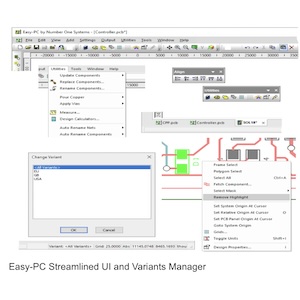
- Application Enhancements: The updated user interface includes a new 'flat' look, improved toolbars, and the addition of a Utilities menu to simplify the design experience and increase productivity.
- Library Management and Creation: Enhanced tools for library creation and editing now include support for .epl format files, improved symbol editing, and access to over 15 million ready-to-use components.
- Design and Editing: Powerful new features like flip vertical mode, rotate around center, and text cutout creation for copper layers make designing faster and more intuitive.
- Design Checking and Integrity: Upgraded geometry checks and a reorganized DRC dialog ensure more accurate and stable designs.
- Plotting and Manufacturing: New tools for drill ident creation, automatic plot generation, and enhanced via handling allow for more seamless manufacturing.
Designers using Version 28 will benefit from full compatibility with the latest versions of Windows (10 and 11), access to over 15 million components through the Component Search Engine and over 10 million components via SnapMagic, continued support from a dedicated technical team, and access to supplementary component libraries.
Share on:


Testimonial
"We’re proud to call I-Connect007 a trusted partner. Their innovative approach and industry insight made our podcast collaboration a success by connecting us with the right audience and delivering real results."
Julia McCaffrey - NCAB GroupSuggested Items
Dragonfly Energy Secures Additional Nevada Tech Hub Funding
05/07/2026 | Globe NewswireDragonfly Energy Holdings Corp., an industry leader in energy storage and maker of Battle Born Batteries®, announced it has been selected for a second consecutive round of funding through the Nevada Tech Hub.
Designing Without a Rulebook: When Engineering Becomes Innovation
05/05/2026 | Stephen V. Chavez, Siemens EDAWhat if the very rules that made you successful as a PCB designer are the ones now holding you back? This reminds me of walking the floor and attending sessions at both PCB West 2025 and APEX EXPO 2026, where one common theme stood out: More designs with traditional PCB “best practices” simply don’t apply. It’s not because they’re wrong, but because the problems we’re solving have fundamentally changed. In some cases, those best practices can actually limit performance. This is where PCB design moves beyond optimization and into something far more challenging: designing without a rulebook.
Custom LIDAR Optics Support Mission-Critical Performance
05/05/2026 | PRNewswireMeller Optics, Inc. has introduced custom fabricated LIDAR optics that can be engineered for specific UV to IR transmission requirements featured in airborne, ground, and maritime defense systems.
Trouble in Your Tank: In Complex Systems, Design Rules Aren’t Optional
05/06/2026 | Michael Carano -- Column: Trouble in Your TankThere is no question that the electronics industry, especially in circuit board design and fabrication, advanced packaging, and innovation throughout the value chain, has seen a significant transformation, whether it be in materials, system architecture, HDI and ultra HDI, semiconductors, or chiplets. AI and high-performance computing (HPC) are driving change across several fronts, including material properties, assembly techniques (think hybrid bonding), and power management.
EMI Strengthens Test Capability with Acculogic Flying Probe System
05/04/2026 | Express Manufacturing, Inc.Express Manufacturing, Inc. (EMI), a global electronics manufacturing services (EMS) provider, has added the Acculogic Scorpion 980E Flying Probe Test System to its inspection and test operations, giving the company greater flexibility in how it validates and supports today’s increasingly complex electronics.