


 Beyond the Board: How a Diminished Supplier Base Affects Complex PCB Manufacturing Readiness in Defense
 Defense Speak Interpreted: Hypersonics Report Back After Six Years of Silence
 American Made Advocacy: American Microelectronics Power the Future of High Technology


World Record for Tandem Perovskite-CIGS Solar Cell
September 10, 2019 | HZBEstimated reading time: 2 minutes
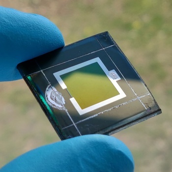
A team headed by Prof. Steve Albrecht from the HZB will present a new world-record tandem solar cell at EU PVSEC, the world's largest international photovoltaic and solar energy conference and exhibition, in Marseille, France on September 11, 2019. This tandem solar cell combines the semiconducting materials perovskite and CIGS and achieves a certified efficiency of 23.26%. One reason for this success lies in the cell’s intermediate layer of organic molecules: they self-organise to cover even rough semiconductor surfaces. Two patents have been filed for these layers.
Perovskite-based solar cells have experienced an incredibly rapid increase in efficiency over the last ten years. The combination of perovskites with classical semiconductor materials such as silicon and copper-indium-gallium-selenide (CIGS) compounds in tandem solar cells promises low-cost, high-performance solar modules for the future. However, losses at the electrodes between the two semiconductors considerably reduce the efficiency.
Record Efficiency: 23.26%
HZB physicist Prof. Steve Albrecht and his team now successfully established novel electrode coatings that greatly reduce these losses. They could produce a monolithic tandem solar cell from perovskite and CIGS that achieved an officially certified efficiency of 23.26%, which currently is a world record value. The tandem cell has an active area of one square centimetre and thus reaches another milestone, as perovskite CIGS tandem cells have so far been significantly smaller.
Self Assembled Monolayer
The contact layers consist of carbazole-based organic molecules coupled to phosphonic acid groups. These molecules arrange themselves into what are known as self-assembled monolayers (SAMs). These SAMs have highly favourable electro-optical properties and the self-assembly even leads to complete coverage of rough semiconductor surfaces.
Two Patents Filed
“The SAMs are strikingly simple and robust. This also allows them to be scaled up to industrial levels. In addition, they are compatible to a wide variety of substrates and their material consumption is extremely low”, explains Amran Al-Ashouri, PhD student in the Albrecht group and first author of the study. This work might further accelerate progress towards extremely inexpensive perovskite-based PV technologies. The group has now filed two patents and is currently in licensing negotiations.
Prof. Steve Albrecht heads the Perovskite Tandem Solar Cells Junior Research Group funded by the German Federal Ministry of Education and Research (BMBF). Work on the perovskite solar cells took place primarily in the Helmholtz HySPRINT Innovation Lab, while the SAMs were developed in close collaboration with Kaunas University of Technology (Lithuania), where the group of Prof. Vytautas Getautis synthesized the molecules. The CIGS layers are provided by the group of Dr. Christian Kaufmann, who heads the high efficiency CIGS activities at HZB and is supported by the SpeedCIGS project funded by the German Federal Ministry for Economic Affairs and Energy (BMWi).
Share on:


Testimonial
"We’re proud to call I-Connect007 a trusted partner. Their innovative approach and industry insight made our podcast collaboration a success by connecting us with the right audience and delivering real results."
Julia McCaffrey - NCAB GroupSuggested Items
Nortech Systems Launches Power over Fiber Technology Platform for EMI-Sensitive Applications
04/08/2026 | Globe NewswireNortech Systems Incorporated, a leading provider of design and manufacturing solutions for complex electromedical devices and electromechanical systems, has announced the launch of its Power over Fiber technology platform.
Flexible Thinking: Designing Flex Circuits for Dynamic Reliability
04/09/2026 | Joe Fjelstad -- Column: Flexible ThinkingFlex circuits flex. No surprises there. However, they are also very commonly designed into products because they are thin and offer consistent thickness and dielectric properties, attributes highly prized by present-day product designers of personal electronics. This would include smartphones and, increasingly, wearable electronics for medical monitoring and even fashion.
Understanding Tolerances in Flexible Circuit Design
04/01/2026 | Chris Clark, Flexible Circuit TechnologiesThe challenge with cumulative tolerances is meeting the dimensional requirements for items dimensioned on a drawing or specification for a flexible or rigid-flex circuit. It is critical to understand the fabrication processes and how features are defined when creating your tolerance requirements.
Target Condition: An Exploration of Flooding PCB Layers
04/02/2026 | Kelly Dack -- Column: Target ConditionThe concept of flooding PCB layers with copper has been around for so long, you’d think we’d have it mastered. We haven’t. (Oh, and by “we,” I mean design engineers and the software tools we depend on.) Years ago, PCB artwork was created by hand using light tables, with tape applied to Mylar. Signals were slow, traces were relatively wide, and high-current paths were simply “beefed up” with wider copper. Signal integrity wasn’t yet a driving concern. Today, solid return paths are fundamental to robust design. We understand the importance of continuous reference planes for signal integrity and EMI control.
New, Greener Solutions for Etch: Novel Copper Extraction
03/30/2026 | Richard Nichols, GreenSource Engineering“Novel” is a typical marketing phrase that implies new and unique, but often “novel” actually means an established technology being applied to a new field or application. This, in turn, is often driven by newly relevant external motivation. GreenSource has been working on just such a solution: novel copper extraction, offering a better and greener alternative to traditional LLE control systems for cupric chloride etch.