


 Trouble in Your Tank: Organic Addition Agents in Electrolytic Copper Plating
 Marcy’s Musings: Can You Hear the Voices?
 Facing the Future: Successfully Navigating the Uncertain Path Ahead


Wild River, eSilicon, and Samtec Team up for 112-Gbps Test Vehicle
June 6, 2019 | Andy Shaughnessy, Design007 MagazineEstimated reading time: 10 minutes
During DesignCon, I sat down for an interview with Tim Horel from eSilicon, Al Neves of Wild River Technology, and Matt Burns from Samtec. They’ve recently teamed up to create a 112-Gbps test vehicle that may be the first of its kind of test fixture.
Andy Shaughnessy: Tim, I understand you all have teamed up to do a test vehicle that’s pretty cutting edge. Can you give us an overview of the whole thing?
Tim Horel: Essentially, what happened was eSilicon acquired a new SerDes organization a few years back and commissioned the team to produce a 56-Gbps SerDes design for our networking and telecommunications space. And we were surprised because the first silicon that came out met specifications and was ready for sale. We were about two quarters ahead of where we had thought we would be and were kind of scrambling.
We had an existing evaluation platform designed for lower data rates, which came from the original company that we had acquired all the rights from; we were looking for a way to upgrade it. We realized that we had the skill set in-house, but they were busy on packaging work, and this is a board. So, we needed a new evaluation platform that would provide all of the capabilities required for the 112-Gbps design, which is coming next.
We were looking for something that would let people easily de-embed the measurements and see if they could achieve really high signal integrity to fully demonstrate the reach of the SERDES solution. For the second phase of evaluation, signal integrity personnel at larger companies had favorite channels that failed various tests over the years, so they begin to use those as standards for new designs. They just take the evaluation board and hook it up to their favorite channels that have a lot of channel pathology, and they determine if you can successfully equalize the channel and achieve good bit error ratio.
Thus, what we really needed was somebody like SEAL Team Six to come in and get me a new board that fixed all of those problems in one shot. I had known about Al’s company Wild River for a long time, and I hadn’t had any reason to engage with him, but I reached out, and we started a conversation and realized that there was a good project there. We collaborated at DesignCon, and one of the things that we needed were connectors to do this job, which ended up coming from Samtec for various other reasons.
We received the first version of the board—the beta version—and it did not meet the fabrication specifications, so it had to be re-spun. But even with that, the board is exceeding performance capabilities of the previous board, so we’re pleased with the result and looking forward to the next version so that we can go wide with it.
Shaughnessy: And you’re at 112 Gbps now?
Horel: The current version is at 56 Gbps, but it has two ports for 56 Gbps and another port for 112 Gbps, so it’s already built into the board. I’ll have that silicon in hand in late August.
Shaughnessy: Al, tell me a little bit about your role in all of this. What did you see when you first became involved? What were your concerns as you looked at it?
Al Neves: Well, there’s a science-fiction comment that’s really appropriate: “In space, everything can kill you.” And when you’re doing work even at 56 Gbps, the requirements of the PAM4 technology for test fixturing is formidable; everything needs to be top-tier SI metrics. There’s a new emerging standard—IEEE P370—that helps with our guidance of that, and we use it along with some simulations as a guide to establish metrics for doing the 3D EM optimization. The 3D EM optimization was the floor plan—the SI of the platform. Most importantly, the crux issue was the high-density interconnect, which was the Bulls Eye connector from Samtec going into the board.
For the electromagnetic simulation, we had two internal teams, and we also used an external Samtec team. Our experience using external teams from connector companies was universally very negative. They’re not usually up to the requirements of the advanced SI that you need for PAM4. However, the Samtec team did a fabulous job. In fact, we used three independent teams—two internal teams using two different tools, and then a Samtec team—and we overlaid all of those. Their results and the Wild River team’s overlaid very closely and the synergy between the teams was really brilliant
The objective in all of that is for everybody to get together and look at the results of that. If there’s an outlier in one of the optimizations, we research it, and if they closely correspond it gives us a lot of confidence. It sounds expensive to have three teams, but in the long run, it produces dramatic cost savings. I don’t know why companies don’t do it more; it’s a boon. And in the time it takes for one person to do it sitting in front of their computer banging out a simulation, if they get it wrong, you have an assembled board that doesn’t work. You have to figure out what’s wrong, redo the optimization, and then lay it out again, refabricate it, reassemble it, and get another team to look at the integrated Serial Link solution, including fiddling with the EQ.
The hassle factor of not getting this right is daunting, and we circumvent all of that by generally having three teams. The Samtec team worked out really well for us, and we were successful. There were some fabrication issues, but for 112 Gbps, there’s always a little bit of cleanup that you need to do to achieve the top-tier SI metric, and that’s Tier 1 of P370, which we’ll achieve on the next spin. We reached the lower metric on the first spin even with the fabrication issue.
Shaughnessy: What’s the board made from?
Neves: That’s a good question. The stackup in materials is no different than what you use to make a fine meal. You have to pick the right materials. The stackup must be well-localized. We use Tachyon 100G, two plies of material strung orthogonally on the glass, and the weave was XY. It’s symmetrical in the X and Y; then, we spread the weave. The stackup for the 112-Gbps version is set so that we get very good localization. A lot of companies are making big mistakes on their stackups, and they’re not just picking the wrong materials; they’re automatically going to the lowest Dk. Instead, we chose materials that lend themselves to strong optimization with the 3D EM in SI. And the board has 12 layers.
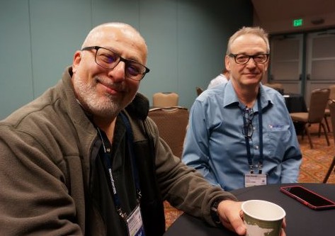
Al Neves, Tim Horel, and Matt Burns discuss their new 112 Gbps test vehicle.
Shaughnessy: How do your connectors fit in here, Matt?
Matt Burns: We looked at this project as an opportunity to work with market leaders like eSilicon and Wild River Technology. This platform presented a unique opportunity for us to release the latest generation of our Bulls Eye test point system. It’s designed as an SMA replacement technology and gives you four times the amount of space savings as well as performance. The second generation of the product provides performance out to 40 GHz, and we’re working closely with eSilicon to move that up to 70GHz for next-generation solutions.
Al talked about the collaboration that Samtec brought to the table. In any connector design setting, we can’t just provide the connector; e have to provide the entire ecosystem of design and support. It’s about the connector and modeling, working with the team to identify the right stackup, breaking out the connector, and making sure the channel is optimized. You have to offer continuous design support whether it’s modeling, simulating, or testing it. This presented us with a nice opportunity for our SI team to work in conjunction with Al and his team to verify the results. The new platform allows not only testing, but for our combined OEM customers, it also enables testing in real-world applications. With the new platform, we’re running 56 Gbps PAM4 over a five-meter XMAX backplane cable solution. When you see a 15–16-foot cable running at those high speeds, it’s the real world.
Shaughnessy: You all use what you’ve learned from this experience to help your customers.
Horel: And one of the interesting thing about this is it’s a five-meter cable. It shows the true long reach capability of the SerDes in that our bit error ratio on this interface is 1e-11 without an FEC—long reach, 56 Gbps, PAM4 series.
Shaughnessy: So, what’s next?
Horel: From eSilicon’s perspective, this board is the evaluation platform anybody who’s going to buy my SerDes will need to use. They’ll put this in their lab, review all of the electrical characteristics, and start playing with their nasty channels for interoperability. But it also authors a reference platform that says, “If you want your system to behave nicely from an electrical point of view, here’s an example of how you do that.”
Burns: Based on the feedback we’ve received so far at DesignCon, including the interest in the solution, demo, and results, we anticipate a lot of follow-up. You’ll see more information from us on additional opportunities to see the system.
Neves: I’m looking forward to driving myself to the local ICU and having a vacation (laughs)!
Shaughnessy: How long have you all been working on this?
Horel: It has been about six months now. These are not short programs.
Neves: It’s what an SI technologist lives for. This is good stuff. One of the things that we’re doing, and the eSilicon people bought into this really early, is this whole concept of reference design. Usually, reference design is code for, “We have something that’s going to help you,” but it’s often very limited in its scope.
And the way that we developed a channel modeling platform that’s co-panelized with the test fixture is novel because it does two things for you. First, you can take the Bulls Eye connector and the associated traces and do very pristine de-embedding, which is part of the compliance specifications. Second, if you want to create your own platform or design with that, we have electromagnetic hooks for doing things like loss modeling, material identification, and modeling of all the vias and transitions in the system. We pulled all of the electromagnetically good pieces of vias, traces, etc., apart, and you’re able to de-embed the jitter when you’re doing the compliance stuff with an oscilloscope.
So, it’s not just helping with the characterization; it’s also helping with post-design activity using a companion channel modeling platform. A lot of our customers say, “I don’t want to do that. I just want to focus on getting a solution as fast as possible.” What I like about this is it can help a customer willing to invest in a full solution.
Horel: And the customers we have want that platform. In previous incarnations of my career, there were groups of companies that I would not give such a platform to because I couldn’t trust them to make the measurements. These customers could use some coaching, and a couple of them are on a similar level to Al; they’re hidden away and nobody lets them out into the sunshine (laughs).
Neves: I didn’t realize I was that much of a recluse (laughs).
Horel: Maybe you’re not a recluse, but that’s why you’re having a hard time finding people to hire (laughs). They put them in a lab, and they lock them up, but this platform will be very useful to them.
Shaughnessy: Do you think this is the first 112-Gbps test vehicle of its kind?
Horel: I don’t know that it’s the first, but it’s certainly one of the cleanest reference platforms for evaluation that I have ever seen.
Burns: Yes, I’d second what Tim just mentioned because of the unique combination of all the features of the kit. It has state-of-the-art silicon from eSilicon. It has best-in-practice and best-in-world SI design and verification. Al also mentioned earlier the inclusion of the IEEE P370 de-embedding technology. When you look at the ecosystem that came together on the platform, it is unique. From that perspective, it is the first in the industry.
Shaughnessy: Thanks a lot, gentlemen. Very impressive.
Neves: Thank you, Andy.
Share on:


Suggested Items
Real Time with... IPC APEX EXPO 2025: Aster–Enhancing Design for Effective Testing Strategies
04/18/2025 | Real Time with...IPC APEX EXPOWill Webb, technical director at Aster, stresses the importance of testability in design, emphasizing early engagement to identify testing issues. This discussion covers the integration of testing with Industry 4.0, the need for good test coverage, and adherence to industry standards. Innovations like boundary scan testing and new tools for cluster testing are introduced, highlighting advancements in optimizing testing workflows and collaboration with other tools.
Real Time with... IPC APEX EXPO 2025: Emerging Trends in Design and Technology
04/16/2025 | Real Time with...IPC APEX EXPOAndy Shaughnessy speaks with IPC design instructor Kris Moyer to discuss emerging design trends. They cover UHDI technology, 3D printing, and optical data transmission, emphasizing the importance of a skilled workforce. The role of AI in design is highlighted, along with the need for understanding physics and mechanics as designs become more complex. The conversation concludes with a focus on enhancing math skills for better signal integrity.
Electronic System Design Industry Posts $4.9 Billion in Revenue in Q4 2024
04/15/2025 | SEMIElectronic System Design (ESD) industry revenue increased 11% to $4,927.3 million in the fourth quarter of 2024 from the $4440.9 million reported in the fourth quarter of 2023, the ESD Alliance, a SEMI Technology Community, announced in its latest Electronic Design Market Data (EDMD) report.
Connect the Dots: Involving Manufacturers Earlier Prevents Downstream Issues
04/17/2025 | Matt Stevenson -- Column: Connect the DotsIf you have read any of my earlier columns, you know I am passionate about helping designers design for the reality of manufacturing. Designing for manufacturability (DFM) is a team sport. DFM is a design process that looks forward to the manufacturing process and integrates with it so that manufacturing requirements and capabilities can be accurately reflected in the design work.
Global PCB Connections: The Next Wave of HDI PCBs– How Design Engineers Can Stay Ahead
04/17/2025 | Jerome Larez -- Column: Global PCB ConnectionsHigh density interconnect (HDI) printed circuit boards have come a long way from their origins as a niche technology for miniaturized applications. Today, HDI PCBs are at the forefront of innovation, driven by an insatiable demand for faster, smaller, and more powerful electronic devices. As consumer electronics, 5G infrastructure, and AI-driven systems advance, design engineers must stay ahead of the curve to ensure their PCB designs meet evolving industry demands.