


 The Right Approach: The Pros and Cons of PCB Vertical Integration
 American Made Advocacy: PCBAA’s Fifth Annual Meeting—Growing Membership and Valuable Relationships
 It's Only Common Sense: Why the Best Years of Electronics Are Still Ahead of Us


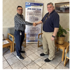
The Training Connection LLC (TTC-LLC) has hired Hermes Gonzalez as a Test Development Engineer, adding deep experience in flying probe and in-circuit test (ICT) to its engineering team.
In this role, Gonzalez will focus on test development for flying probe platforms, including the Seica Pilot V8, as well as ICT development on the Keysight 3070. His addition supports TTCI’s ongoing work in delivering test solutions for complex, high-reliability electronics.
Gonzalez brings more than 15 years of experience in test engineering, with a background that spans aerospace, defense, and high-performance electronics. He has led test development efforts for complex RF PCBAs, supporting new product introduction (NPI), production ramp, and continuous improvement initiatives. His work has included developing flying probe test programs, implementing ICT systems, and working closely with design teams to improve test coverage and manufacturability.
Prior to joining TTCI, Gonzalez held senior test engineering roles at companies including BAE Systems and CesiumAstro, where he was responsible for deploying and optimizing test platforms such as flying probe systems and Keysight 3070 ICT. His experience includes debugging complex circuit failures to the component level, improving test efficiency, and reducing false failures in production environments.
“Hermes brings a strong mix of hands-on test development and real-world production experience,” said Bert Horner, President of TTCI. “He understands how to build test solutions that not only work in development, but hold up in production.”
TTCI specializes in electronic test engineering services, including in-circuit test (ICT), flying probe test (FPT), boundary scan (JTAG), functional test development, and design for test (DfT). By adding Gonzalez to the team, the company further strengthens its ability to support customers with complex assemblies, faster program ramp-up, and improved test coverage.
With growing demand for flexible and scalable test solutions, Gonzalez’s experience in both flying probe and ICT platforms will help TTCI continue to support customers across aerospace, defense, medical, and other high-reliability markets.


