


 It’s Only Common Sense: If You’re Not Differentiated, You’re Dead
 Alpha Insights, Performance by Design: The Future of PCB Manufacturing in the Midwest
 Happy’s Tech Talk #43: Engineering Statistics Training With Free Software


Koh Young Showcases Advanced Dimensional Metrology and Inspection Solutions for Semiconductor and Wafer-Level Packaging at SEMICON West
September 3, 2025 | Koh YoungEstimated reading time: 1 minute
Koh Young Technology, the industry leader in True 3D™ measurement-based dimensional metrology and inspection solutions, will present its latest advancements for semiconductor and advanced packaging applications at SEMICON West 2025 in Booth 5949. The show will take place in its new venue at the Phoenix Convention Center from October 7–9, 2025 in Phoenix, Arizona.
With nearly 25,000 systems installed at more than 3,900 manufacturing sites, Koh Young set the standard in automated optical inspection for the electronics manufacturing industry. Building on that foundation, the company expanded into semiconductor manufacturing with higher-resolution optics, advanced measurement algorithms, and solutions engineered for metrology and inspection of wafer-level packages (WLP), system-in-package (SiP), and ultra–high-density interconnect applications.
As an exhibitor, Koh Young will highlight how its AI-powered metrology and inspection solutions help manufacturers meet the exacting demands of advanced packaging and semiconductor processes. From wafer-level to SiP, Koh Young technology delivers accurate, repeatable data to enable smarter process control, drive higher yields, and support zero-defect initiatives.
Proven Platforms for Advanced Packaging Metrology
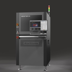
Koh Young’s Meister Series is purpose-built for advanced packaging, including SiP, WLP, and die-stacking metrology. These systems provide ultra-high-resolution 2D/3D measurement to manage features and tolerances in next-generation designs. Complementing the Meister Series, the ZenStar delivers wafer-level dimensional metrology to detect and quantify critical parameters at the earliest stage, ensuring only known-good components advance. Together, these platforms help manufacturers maintain tight process windows, improve yield, and reduce costly rework.
“We are excited about the opportunities SEMICON West brings this year in Phoenix,” said Joel Scutchfield, General Manager of Koh Young America. “The region has long been a center for semiconductor manufacturing, and the recent wave of investment and expansion has only strengthened its position as a hotbed for advanced packaging and innovation. We see tremendous potential for Koh Young to help manufacturers here solve their most pressing challenges. Our mission is to deliver meaningful process insights that improve yield, reduce risk, and give our customers a competitive edge. This show is the perfect forum to collaborate and share how our metrology and inspection solutions can make that vision a reality.”
Share on:


Testimonial
"The I-Connect007 team is outstanding—kind, responsive, and a true marketing partner. Their design team created fresh, eye-catching ads, and their editorial support polished our content to let our brand shine. Thank you all! "
Sweeney Ng - CEE PCBSuggested Items
Advanced Semiconductor Packaging Market Sees Rising Adoption Across Automotive and Industrial Sectors
10/14/2025 | openPRThe semiconductor packaging market size is estimated to reach at a CAGR of 7.2% during the forecast period (2024-2031).
SEMICON West: The Path to a $1 Trillion Future
10/14/2025 | Marcy LaRont, I-Connect007After more than 50 years in San Francisco, SEMICON West moved its 2025 show to Phoenix, which is significant because it highlights the importance of Arizona as a semiconductor and tech hub. Though the show will be back in San Francisco in 2026, the overwhelmingly warm welcome SEMI received from Arizona Governor Katie Hobbs, Phoenix Mayor Kate Gallego, and ASU President Michael Crowe—who has been responsible for ASU repeatedly achieving the U.S. News and World Reports most innovative university ranking—was remarked upon repeatedly. All indications are that SEMICON West may well be back in Phoenix after that 2026 season.
Is Glass Finally Coming of Age?
10/13/2025 | Nolan Johnson, I-Connect007Substrates, by definition, form the base of all electronic devices. Whether discussing silicon wafers for semiconductors, glass-and-epoxy materials in printed circuits, or the base of choice for interposers, all these materials function as substrates. While other substrates have come and gone, silicon and FR-4 have remained the de facto standards for the industry.
Thallner Recognized for Leadership and Innovation in Semiconductor Equipment and MEMS Manufacturing
10/10/2025 | SEMISEMI, the industry association serving the global semiconductor and electronics design and manufacturing supply chain, announced Erich Thallner, President and Co-founder of EV Group (EVG), as its first SEMI Americas Catalyst Award recipient at SEMICON West 2025.
I-Connect007 Editor’s Choice: Five Must-Reads for the Week
10/10/2025 | Nolan Johnson, I-Connect007I-Connect007 has a new monthly digest newsletter, the Advanced Electronic Packaging Digest, and as I was scanning our advanced packaging newsfeeds this week, I came across a primer from tokenring.ai (republished through station WRAL, Raleigh, North Carolina), which I found quite useful. Whether you’re a designer, fabricator, or assembler, the package schemes being developed will change how you work, so be sure to keep your eye on the technological horizon and subscribe to the monthly Advanced Electronic Packaging Digest.