


 It’s Only Common Sense: If You’re Not Differentiated, You’re Dead
 Alpha Insights, Performance by Design: The Future of PCB Manufacturing in the Midwest
 Happy’s Tech Talk #43: Engineering Statistics Training With Free Software


SK keyfoundry, in Collaboration with LB Semicon, Co-Develops Direct RDL to Advance Semiconductor Packaging
July 21, 2025 | SK keyfoundryEstimated reading time: 2 minutes
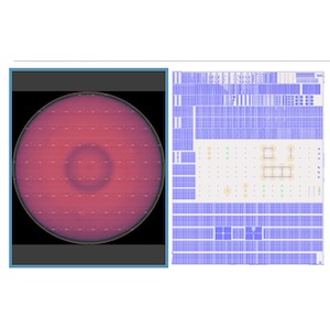
SK keyfoundry, an 8-inch pure-play foundry in Korea, announced that it has successfully co-developed core technology and completed reliability testing of Direct RDL (Redistribution Layer) – a core semiconductor packaging technology based on 8-inch wafers – in collaboration with LB Semicon. This achievement marks a significant step forward in advancing next-generation semiconductor packaging technologies and strengthening the competitiveness of automotive semiconductor products.
RDL refers to metal wiring and insulating layers on top of semiconductor chips to enable electrical connections. It is primarily used in WLP (Wafer Level Packaging) and FOWLP (Fan-Out Wafer Level Packaging) processes to enhance connectivity between the chip and the substrate while minimizing signal interference. The newly co-developed Direct RDL by SK keyfoundry and LB Semicon supports power semiconductors with high current capacity, outperforming competitors. The technology achieves a metal wiring thickness of up to 15 μm and wiring density covering up to 70% of the chip area – making it suitable not only for mobile and industrial applications but also for automotive use. In particular, the solution meets the Auto Grade 1 classification under AEC-Q100 international automotive semiconductor quality standard, ensuring reliable operation in harsh environments with an operating temperature range of –40℃ to +125℃. Unlike competitors, this makes the technology fully viable for automotive products. In addition, by providing a Design Guide and Process Development Kit, SK keyfoundry can now offer a process solution tailored to customer needs, enabling smaller chip sizes, lower power consumption, and cost-effective packaging.
Semiconductor packaging and testing specialist LB Semicon stated that leveraging SK keyfoundry’s deep understanding of semiconductor processes and advanced manufacturing capabilities significantly shortened the development timeline. Through the integration of its own back-end processing technologies with SK keyfoundry’s foundry process expertise, the two companies successfully achieved optimized wafer-level Direct RDL formation, which is expected to greatly enhance production efficiency.
LB Semicon’s CEO Namseog Kim commented, “The joint development of direct RDL has served as an important milestone in strengthening the technological competitiveness of SK keyfoundry and LB Semicon.” He also added, “Through close collaboration between the two companies, we plan to establish a strong foothold in the next-generation semiconductor packaging market, built on high reliability.”
“The joint development with LB Semicon, the semiconductor packaging specialist, holds significant meaning as it demonstrates the successful integration of our company’s advanced and comprehensive manufacturing expertise into cutting-edge semiconductor packaging process development,” said Derek D. Lee, CEO of SK keyfoundry. “SK keyfoundry will continuously collaborate with LB Semicon, a leading company in semiconductor technology, to further evolve and position ourselves as a premier foundry with proven capabilities in delivering high-performance and high-reliability semiconductor solutions to the global market.”
Share on:


Testimonial
"Advertising in PCB007 Magazine has been a great way to showcase our bare board testers to the right audience. The I-Connect007 team makes the process smooth and professional. We’re proud to be featured in such a trusted publication."
Klaus Koziol - atgSuggested Items
Is Glass Finally Coming of Age?
10/13/2025 | Nolan Johnson, I-Connect007Substrates, by definition, form the base of all electronic devices. Whether discussing silicon wafers for semiconductors, glass-and-epoxy materials in printed circuits, or the base of choice for interposers, all these materials function as substrates. While other substrates have come and gone, silicon and FR-4 have remained the de facto standards for the industry.
Thallner Recognized for Leadership and Innovation in Semiconductor Equipment and MEMS Manufacturing
10/10/2025 | SEMISEMI, the industry association serving the global semiconductor and electronics design and manufacturing supply chain, announced Erich Thallner, President and Co-founder of EV Group (EVG), as its first SEMI Americas Catalyst Award recipient at SEMICON West 2025.
I-Connect007 Editor’s Choice: Five Must-Reads for the Week
10/10/2025 | Nolan Johnson, I-Connect007I-Connect007 has a new monthly digest newsletter, the Advanced Electronic Packaging Digest, and as I was scanning our advanced packaging newsfeeds this week, I came across a primer from tokenring.ai (republished through station WRAL, Raleigh, North Carolina), which I found quite useful. Whether you’re a designer, fabricator, or assembler, the package schemes being developed will change how you work, so be sure to keep your eye on the technological horizon and subscribe to the monthly Advanced Electronic Packaging Digest.
Marco Pieters Appointed ASML Chief Technology Officer
10/09/2025 | ASMLASML Holding NV (ASML) announced the appointment of Marco Pieters as Executive Vice President and Chief Technology Officer, reporting to President and Chief Executive Officer, Christophe Fouquet.
SEMI Reports Global 300mm Fab Equipment Spending Expected to Total $374 Billion Over Next Three Years
10/09/2025 | SEMIGlobal 300mm fab equipment spending is expected to reach $374 billion from 2026 to 2028, SEMI reported today in its latest 300mm Fab Outlook.