


 It’s Only Common Sense: If You’re Not Differentiated, You’re Dead
 Alpha Insights, Performance by Design: The Future of PCB Manufacturing in the Midwest
 Happy’s Tech Talk #43: Engineering Statistics Training With Free Software


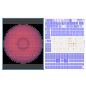
Infineon Advances on 300-millimeter GaN Manufacturing Roadmap as Leading Integrated Device Manufacturer (IDM)
July 10, 2025 | InfineonEstimated reading time: 2 minutes
As the demand for gallium nitride (GaN) semiconductors continues to grow, Infineon Technologies AG is poised to capitalize on this trend and solidify its position as a leading Integrated Device Manufacturer (IDM) in the GaN market. The company announced that its scalable GaN manufacturing on 300-millimeter wafers is on track. With first samples available for customers as of the fourth quarter of 2025, Infineon is well-positioned to expand its customer base and reinforce its position as a leading GaN powerhouse.
As a leader in power systems, Infineon is mastering all three relevant materials: silicon (Si), silicon carbide (SiC) and gallium nitride. With higher power density, faster switching speeds, and lower power losses, GaN semiconductors enable smaller designs, reducing energy consumption and heat generation in electronic devices like smartphone chargers, industrial and humanoid robots or solar inverters.
“Our fully scaled-up 300-millimeter GaN manufacturing will allow us to deliver highest value to our customers even faster while moving towards cost parity for comparable silicon and GaN products,” said Johannes Schoiswohl, Head of GaN Business Line at Infineon. “Almost a year after the announcement of Infineon’s breakthrough in 300-millimeter GaN wafer technology, we are pleased that our transition process is well on track and that the industry has recognized the importance of Infineon’s GaN technology enabled by the strength of our IDM strategy.”
Infineon’s manufacturing strategy primarily relies on an IDM model – owning the entire semiconductor production process, from design to manufacturing and selling the final product. The company’s in-house manufacturing strategy is a key differentiator in the market providing several advantages such as high-quality, faster time-to-market as well as superior design and development flexibility. Infineon is committed to supporting its GaN customers and can scale capacity to meet their needs for reliable GaN power solutions.
Building on its technology leadership, Infineon has become the first semiconductor manufacturer to successfully develop 300-millimeter GaN power wafer technology within its existing high-volume manufacturing infrastructure. Chip production on 300-millimeter wafers is technically more advanced and significantly more efficient compared to established 200-millimeter wafers, as the larger wafer diameter allows 2.3 times more chips to be produced per wafer. These increased capabilities combined with Infineon’s large team of GaN experts and the industry’s broadest IP portfolio are needed as GaN power semiconductors are being rapidly adopted in industrial, automotive, consumer, and computing & communication applications, such as power supplies for AI systems, solar inverters, chargers and adapters or motor control systems.
Share on:


Testimonial
"Our marketing partnership with I-Connect007 is already delivering. Just a day after our press release went live, we received a direct inquiry about our updated products!"
Rachael Temple - AlltematedSuggested Items
Imec Launches 300mm GaN Program to Develop Advanced Power Devices and Reduce Manufacturing Costs
10/13/2025 | ImecImec, a world-leading research and innovation hub in nanoelectronics and digital technologies, welcomes AIXTRON, GlobalFoundries, KLA Corporation, Synopsys, and Veeco as first partners in its 300mm gallium-nitride (GaN) open innovation program track for low- and high-voltage power electronics applications.
Renesas Powers 800 Volt Direct Current AI Data Center Architecture with Next-Generation Power Semiconductors
10/13/2025 | RenesasRenesas Electronics Corporation, a premier supplier of advanced semiconductor solutions, announced that it is supporting efficient power conversion and distribution for the 800 Volt Direct Current power architecture announced by NVIDIA, helping fuel the next wave of smarter, faster AI infrastructure.
SEMI Reports Global 300mm Fab Equipment Spending Expected to Total $374 Billion Over Next Three Years
10/09/2025 | SEMIGlobal 300mm fab equipment spending is expected to reach $374 billion from 2026 to 2028, SEMI reported today in its latest 300mm Fab Outlook.
Advanced Rework Technology Inspires Students at National Manufacturing Day 2025
10/08/2025 | A.R.T. Ltd.Advanced Rework Technology Ltd. (A.R.T.), a leading independent IPC-accredited training provider, joined forces with Jaltek, a UK-based electronics manufacturer with over 35 years’ experience in designing and producing high-quality electronic products, to deliver hands-on workshops for students during National Manufacturing Day 2025.
I-Connect007 Releases Episode 5 of Groundbreaking Ultra HDI Podcast Series
10/10/2025 | I-Connect007In Episode 5 “Via Structures,” host Nolan Johnson welcomes back John Johnson, Director of Quality and Advanced Technology at American Standard Circuits. Together, they explore the designer’s perspective on UHDI’s impact on via structures, diving into the metallurgy, chemistry, mechanical considerations, and stackup reduction that provide greater design flexibility and fewer constraints than ever before.