


 The Right Approach: Get Ready for ISO 9001 Version 6
 Dan’s Biz Bookshelf: ‘Still Broke: Walmart’s Remarkable Transformation'
 Driving Innovation: Depth Routing Processes—Achieving Unparalleled Precision in Complex PCBs


Orbel Corporation Integrates Schmoll Direct Imaging
June 4, 2025 | Schmoll AmericaEstimated reading time: 2 minutes
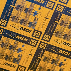
Orbel Corporation in Easton, PA, proudly becomes the first PCM facility in the U.S. equipped with Schmoll’s MDI Direct Imaging system. This installation empowers Orbel to support customers with greater precision and quality.
Key benefits include:
- Compact Design: Easily replaces older units without increasing cleanroom footprint.
- Granite Stability: Ensures precision for high-accuracy demands.
- Automation: Reduces operator inputs and maximizes efficiency.
- Advanced Imaging: Automatic target recognition, even on challenging surfaces (RGB+IR Combi Ringlight).
- Superior Alignment: UV-Marker system for precise front-to-back alignment.
- Optimal Etch Quality: High-res photohead for straight sidewall profiles, tuned to specific photoresist.
"The MDI Direct Imaging system from Schmoll has made a real impact on our production capabilities. We’re seeing faster turnarounds and more consistent results across the board. From design input to the final printed image, everything moves quicker and more smoothly. The automatic alignment feature has noticeably enhanced our accuracy, and being able to serialize each product adds both value and enhancing traceability to our workflow," shared members of the Orbel team. " The system also gives us detailed production logs, which have improved how we monitor and manage our operations. Most importantly, we’re seeing more uniform, repeatable quality—which means higher yields and greater overall efficiency."
They went on to state, "What stood out to us right away was the improved image quality. The level of detail and consistency we can now achieve is simply on another level. This has had a noticeable impact on our end product, especially in applications requiring tight tolerances and sharp feature definition."
The Schmoll MDI system utilizes advanced photohead technology, combining a powerful UV-LED light source with a DMD (Digital Micromirror Device) chip to generate high-resolution images.
The DMD chip itself consists of millions of micromirrors whose precise orientation controls the direction of the UV light, effectively shaping the projected image. This technology enables the transfer of intricate design features onto photosensitive resist materials.
To ensure the stability and definition of these imaged features, the system allows for adjustment of the needed wavelength ratio used during exposure. Operating across multiple UV wavelengths, the MDI system can be finely tuned to accommodate a wide range of photoresists and substrate materials. This broad compatibility makes it a highly versatile and flexible imaging solution for diverse manufacturing requirements.
The team commented, “Having this kind of imaging power on the production floor gives us more confidence in what we deliver. It’s not just about meeting specs, it’s about exceeding expectations."
The Schmoll and Orbel partnership is a strong example of how modern manufacturing technology, backed by effective collaboration and expertise, can drive real progress.
From the initial conversations to the final installation, the partnership between Orbel, Schmoll America, and Schmoll Maschinen Germany was built on open communication, trust and a shared vision for innovation. Each team brought its own strengths to the table, localized support and responsiveness from Schmoll America, deep technical know-how from Germany, and Orbel’s forward-thinking approach to adopting advanced technology.
By working closely together at every stage, from sample testing to operator training, we ensured a smooth implementation of direct imaging technology. The result: faster ramp-up, minimized downtime, and a system running at full potential from day one.
This collaboration reflects what’s possible when the right partners come together with a common goal: pushing manufacturing forward through smart, connected solutions.
Share on:


Testimonial
"The I-Connect007 team is outstanding—kind, responsive, and a true marketing partner. Their design team created fresh, eye-catching ads, and their editorial support polished our content to let our brand shine. Thank you all! "
Sweeney Ng - CEE PCBSuggested Items
United Electronics Corporation Unveils Revolutionary CIMS Galaxy 30 Automated Optical Inspection System
09/11/2025 | United Electronics CorporationUnited Electronics Corporation (UEC) today announced the launch of its new groundbreaking CIMS Galaxy 30 Automated Optical Inspection (AOI) machine, setting a new industry standard for precision electronics manufacturing quality control. The Galaxy 30, developed and manufactured by CIMS, represents a significant leap forward in inspection technology, delivering exceptional speed improvements and introducing cutting-edge artificial intelligence capabilities.
IPS, SEL Raise the Bar for ENIG Automation in North America
09/11/2025 | Mike Brask, IPSIPS has installed a state-of-the-art automated ENIG plating line at Schweitzer Engineering Laboratories’ PCB facility in Moscow, Idaho. The 81-foot, fully enclosed line sets a new standard for automation, safety, and efficiency in North American PCB manufacturing and represents one of the largest fully enclosed final finish lines in operation.
Smart Automation: Odd-form Assembly—Dedicated Insertion Equipment Matters
09/09/2025 | Josh Casper -- Column: Smart AutomationLarge, irregular, or mechanically unique parts, often referred to as odd-form components, have never truly disappeared from electronics manufacturing. While many in the industry have been pursuing miniaturization, faster placement speeds, and higher-density PCBs, certain market sectors are moving in the opposite direction.
Machvision Leads Shift to Automated Inline Final Inspection, AOI in North America
09/10/2025 | Ralph Jacobo, all4-PCBSchweitzer Engineering Laboratories (SEL) chose Machvision inspection equipment due to its capabilities and versatility. Machvision of Taiwan offers circuit inspection, hole inspection and measurement, IC Substrate and HDI inspection, and final visual inspection solutions. The best fit for SEL was the 4.0Pro Circuit Inspection for inner and outer layers, and the AFI6 for final visual inspection of finished panels.
Closing the Loop on PCB Etching Waste
09/09/2025 | Shawn Stone, IECAs the PCB industry continues its push toward greener, more cost-efficient operations, Sigma Engineering’s Mecer System offers a comprehensive solution to two of the industry’s most persistent pain points: etchant consumption and rinse water waste. Designed as a modular, fully automated platform, the Mecer System regenerates spent copper etchants—both alkaline and acidic—and simultaneously recycles rinse water, transforming a traditionally linear chemical process into a closed-loop system.