


 Dan’s Biz Bookshelf ‘House of Huawei'
 Happy’s Tech Talk #41: Sustainability and Circularity for Electronics Manufacturing
 Facing the Future: Challenges and Opportunities in Reshoring PCB Manufacturing


Deca Announces Agreement with IBM to Bring High-Density Fan-Out Interposer Production to North America
May 20, 2025 | Deca TechnologiesEstimated reading time: 1 minute
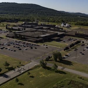
Deca Technologies announced the signing of an agreement with IBM to implement Deca’s M-Series™ and Adaptive Patterning® technologies in IBM’s advanced packaging facility in Bromont, Quebec. Through the agreement, IBM will implement a high-volume manufacturing line with a focus on Deca’s M-Series Fan-out Interposer Technology (MFIT™).
This collaboration builds on IBM’s strategy to develop its advanced packaging capabilities. IBM Canada's plant in Bromont is one of North America’s largest semiconductor assembly and test sites and has been at the forefront of packaging innovation for over five decades. Recent investments to expand the site’s capabilities have positioned it as a critical hub for high-performance packaging and chiplet integration, supporting technologies like MFIT that are essential for AI, HPC, and data center applications.
Deca’s M-Series platform is the highest-volume fan-out packaging technology in the world, with over seven billion M-Series units shipped. MFIT builds on this proven foundation by integrating embedded bridge die for chips’ last processor and memory integration delivering high-density, low-latency connections between chiplets. MFIT provides a cost-effective alternative to full silicon interposers, offering improved signal integrity, greater design flexibility, and the scalable format needed for ever-larger AI, HPC, and data center devices.
This cooperation reflects the shared commitment of IBM and Deca to advance the next generation of semiconductor packaging. By combining IBM’s advanced packaging capabilities with Deca’s proven technology, the two companies are expanding the global supply chain for the future of high-performance chiplet integration and advanced computing systems.
“Advanced packaging and chiplet technology are critical for faster, more efficient computing solutions in the age of AI. Deca will help ensure IBM’s Bromont facility remains at the forefront of these innovations, strengthening our commitment to helping our clients bring products to market faster and deliver better performance for AI and data-heavy applications,” said Scott Sikorski, Head of Business Development for Chiplets & Advanced Packaging at IBM.
“IBM’s rich history in semiconductor innovation and advanced packaging makes them an ideal partner to bring MFIT to high-volume production,” said Tim Olson, Founder and CEO of Deca. “We are thrilled to be working together to bring this advanced interposer technology to the North American ecosystem.”
Share on:


Testimonial
"We’re proud to call I-Connect007 a trusted partner. Their innovative approach and industry insight made our podcast collaboration a success by connecting us with the right audience and delivering real results."
Julia McCaffrey - NCAB GroupSuggested Items
Koh Young Showcases Advanced Dimensional Metrology and Inspection Solutions for Semiconductor and Wafer-Level Packaging at SEMICON India
08/14/2025 | Koh YoungKoh Young, the industry leader in True 3D™ measurement-based dimensional metrology and inspection solutions, will present its latest advancements for semiconductor and advanced packaging applications in Hall 1 Booth 1086 during SEMICON India 2025 held September 2-4, 2025, at Yashobhoomi (IICC), New Delhi, India.
Koh Young Highlighting Dimensional Metrology & Inspection Solutions at the Binghamton University Electronics Packaging Symposium
08/12/2025 | Koh YoungKoh Young, the industry leader in True 3D™ measurement-based dimensional metrology and inspection solutions, is proud to announce its sponsorship and participation in the 36th Annual Electronics Packaging Symposium (EPS), hosted at the GE Aerospace Research Campus in Niskayuna, New York, on September 03-04, 2025.
Inside the AI Hardware Boom: Servers, Substrates and Advanced Packaging
08/07/2025 | Edy Yu, Printed Circuit Information, China, and Marcy LaRont, I-Connect007AI is rewriting the hardware playbook, marrying complex software and algorithms to run and improve machine and equipment operations. Sorting through, managing, and utilizing massive amounts of data takes tremendous data storage and processing power. Enter the new generation of supercomputers and data servers. The data servers being built today are not your momma’s server, as they say.
ASMPT Earns Global Recognition for Outstanding Customer Service in 2025 TechInsights Survey
07/31/2025 |ASMPT has been recognised for excellence in the 2025 TechInsights Global Semiconductor Supplier Survey for the 12th consecutive year. This year, it was ranked third for excellence in customer service among large equipment suppliers.
Libra Industries Launches In-House High Precision Underfill Capabilities
07/17/2025 | Libra IndustriesLibra Industries, a leading provider of systems integration and electronics manufacturing services (EMS), is excited to announce the addition of high-precision underfill to its in‑house manufacturing capabilities.