


 Trouble in Your Tank: Understanding Interconnect Defects, Part 1
 It’s Only Common Sense: Marketing Isn’t Fluff, It’s Ammunition
 Driving Innovation: Mechanical and Optical Processes During Rigid-flex Production


imec Inks MoU with the intention to Establish New 300mm R&D Process Line in Spain for Specialized Chip Technologies
March 20, 2024 | ImecEstimated reading time: 1 minute
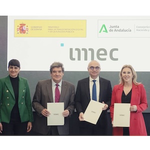
The Spanish government, together with the regional government of Andalusia and imec, a world-leading research and innovation hub in nanoelectronics and digital technology, announced that they have signed a Memorandum of Understanding (MoU) outlining their intent to establish a specialized chip technology pilot line in Malaga (Andalusia). The new innovation facility intends to complement imec’s existing 300mm advanced CMOS process line in Leuven, Belgium, with new 300mm processes developments and the introduction of new materials that are difficult to combine today with standard CMOS processes. The new facility aims to answer the industry’s need for R&D, prototyping and pave the road to the manufacturing of promising, new technologies.
The facility aims to leverage the unique advantages of leading-edge 300mm semiconductor process technology to drive new applications in health care, life sciences, photonics, augmented and virtual reality, precision sensing, ... Complementing the existing expertise and infrastructure in Leuven with non-standard processes that are currently incompatible with semiconductor manufacturing processes, the two sites are meant to be closely linked.
The negotiations will now start with an eye to finding a strong public-private cooperation model, between imec, the Spanish government and the government of Andalusia. The governments already agree to support the construction of the new facility including the advanced equipment. They have also formulated the intention to financially support the pilot line’s operations in a sustainable, long-term manner, to the benefit of its growing semiconductor ecosystem. Imec intends to manage the operations, provide the required knowledge and technology, and guarantee access to its global academic and industrial partner network.
This MoU emphasizes the partners’ ambition to collaborate on a pan-European scale to contribute to the Spanish semiconductor ecosystem. It builds on local strengths, yet leverages cross-border expertise and capabilities to address global societal challenges, while supporting regional economic ambitions. By establishing this new facility, which is closely connected to imec's Leuven-based 300mm pilot line, the goal is to fully harness the innovation potential in Spain and Andalusia. Further details of the operations of the facility, such as hiring prospects, cannot be confirmed yet as they will be concluded in ensuing discussion.
Share on:


Testimonial
"Your magazines are a great platform for people to exchange knowledge. Thank you for the work that you do."
Simon Khesin - Schmoll MaschinenSuggested Items
Automation Meets Sustainability
09/08/2025 | Rick Nichols, GreenSource EngineeringGreenSource Engineering (GSE) is proud to have contributed to the first successful reshoring of a PCB facility on a greenfield site in the United States. While we are honored to have played a key role, full credit for this achievement goes to SEL for its vision, commitment, and professionalism.
TTM Technologies: Bridging East and West with Strategic Expansion
08/25/2025 | Marcy LaRont, I-Connect007As global supply chains shift and demand for supply chain resiliency grows, TTM Technologies is expanding with purpose: bolstering its U.S. presence while maintaining a strong footprint in Asia. With recent moves in Wisconsin and Malaysia, the company is positioning itself to better support customers amid an evolving geopolitical landscape. In this interview, President and CEO of TTM Technologies Tom Edman discusses TTM’s expansion strategy, the future of manufacturing, and his planned retirement after his long tenure at the helm of the company.
Marcy’s Musings: Continuing to Invent the Future With SEL
08/19/2025 | Marcy LaRont -- Column: Marcy's MusingsTwo years ago, PCB007 Magazine devoted an issue to Schweitzer Engineering Labs (SEL), a new captive greenfield PCB facility in Moscow, Idaho. We highlighted some of the most cutting-edge achievements in facility layout, design, and equipment in the PCB fabrication industry. SEL was a shining example of what was possible, providing insight and inspiration to PCB fabricators looking toward growth and expansion.
August 2025 PCB Magazine: Inventing the Future With SEL
08/18/2025 | I-Connect007 Editorial TeamTwo years after launching its state-of-the-art PCB facility, Schweitzer Engineering Laboratories shares lessons in vision, execution, and innovation, plus insights from industry icons and technology leaders shaping the future of PCB fabrication. The August 2025 issue of PCB007 Magazine takes you inside the facility to hear from its founder, Dr. Ed Schweitzer, its manufacturing team leaders, and several of the supplier vendors that make this a cutting-edge fabrication plant.
Polymatech Electronics Limited Announces Completion of PCB Manufacturing Facility in Europe
08/15/2025 | PR NewswirePolymatech Electronics Limited is thrilled to announce the successful commissioning of its state-of-the-art Printed Circuit Board (PCB) manufacturing facility in Estonia, Europe. This milestone represents a significant advancement in the company's strategic expansion across the European market.