


 The Marketing Minute: A Brand Visibility Playbook—Get Seen, Heard, and Remembered
 American Made Advocacy: Supporting the Entire PCB Ecosystem—Materials to OEMs
 Marcy's Musings: The Hole Truth—Via Integrity in an HDI World


Researchers Discovered New Method for Improving Perovskite Solar Cell Performance
June 22, 2017 | Aalto UniversityEstimated reading time: 2 minutes
The Aalto-developed treatment builds on previous breakthroughs improving the efficiency and longevity of perovskite solar cells using established printing methods (carbon back contact based perovskite solar cells or CPSCs). These findings make it possible to further enhance the efficiency of these types of solar cells.
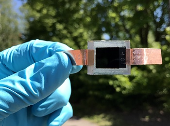
A humidity assisted and thermal treated (HTE) carbon-based printed perovskite solar cell. Photo: Ghufran Hashmi.
Perovskite solar cells are solar cells where the light harvesting layer consists of lead halide with perovskite crystal structure. Globally, perovskite cells are studied intensively since they might prove to be an alternative to silicon cells that require a lot of energy in the manufacturing process.
In the new method, the perovskite solar cells were exposed to 40-degrees in a chamber where humidity was kept in the level of 70% (±5%). This kind of environment normally degrades the properties of perovskite solar cells. In this case, the treatment led to surprising growth of the perovskite crystals, which naturally absorb sunlight and generate electricity.
“The photovoltaic performance was significantly enhanced, and the overall efficiency increased almost 45%,” says Dr Ghufran Hashmi, an Academy of Finland postdoctoral researcher.
“Ghufran Hashmi was interested in possible changes in the atomic structure of the perovskite solar cells. With the state-of-the-art X-ray diffractometer of the Nanomicroscopy Center at Aalto, we were able to monitor the crystallite structure of the perovskite layer before and after the treatment,” says Dr Ulla Vainio, a staff scientist in the Department of Applied Physics, who assisted Hashmi with collecting experimental data.
The team did not stop there, but examined the perovskites using a scanning electron microscopy (SEM). “The SEM images supported the previous observations obtained from the X-ray diffraction method analysis, which endorsed the gradual crystal growth over the period of exposure,” reports Dr Teemu Sarikka, a staff scientist in the Department of Mechanical Engineering.
The task of physics doctoral student Teemu Myllymäki was to check if any chemical changes occurred in the perovskite crystal structure induced by the moisture generated by the thermo-humid environment. In his research, Myllymäki utilized Fourier transform infrared spectroscopy (FTIR). “The comparison between the fresh and exposed solar cells revealed almost no change in the chemical structure of the perovskite light absorbing layer, which endorses the successful implementation of this new treatment method,” he reports.
Solar cells are part of the rapidly expanding area of next-generation, low-cost photovoltaic systems. The team at Aalto benefited from working with collaborators in Switzerland, the Solaronix company and the Swiss Federal Institute of Technology (EPFL) in Lausanne. “Solaronix provided the samples and EPFL researcher Dr Ibrahim Dar helped us in key processes that are critically required for the successful commercialization of this low cost solar cell technology,” says Dr Hashmi.
The team from Aalto University involved in this research work with an HTE treated carbon based printed perovskite solar cell. From left to right: Teemu Myllymäki, Ghufran Hashmi, Ulla Vainio, Teemu Sarikka. Photo: Nonappa.
Share on:


Suggested Items
Sierra Circuits Boosts High Precision PCB Manufacturing with Schmoll Technology
06/16/2025 | Schmoll MaschinenSierra Circuits has seen increased success in production of multilayer HDI boards and high-speed signal architectures through the integration of a range of Schmoll Maschinen systems. The company’s current setup includes four MXY-6 drilling machines, two LM2 routing models, and a semi-automatic Optiflex II innerlayer punch.
Elementary, Mr. Watson: PCB Routing: The Art—and Science—of Connection
06/11/2025 | John Watson -- Column: Elementary, Mr. WatsonMany people who design circuit boards love the routing part of the design. This is partially because we want to stop looking at the annoying rat's nest of connections, which seem to have no rhyme or reason at first glance. We want to get to something more exciting. Routing is the ultimate part of solving the puzzle. You take all the messy lines from the schematic and turn them into neat, organized paths.
Connect the Dots: Proactive Controlled Impedance
05/29/2025 | Matt Stevenson -- Column: Connect the DotsFrom data centers to smartphones, designers know that the ohms have it. Getting impedance right ensures all-important signal integrity and delivers high-performing boards. Our designers understand the importance of controlled impedance, but not everyone addresses it in their designs. The most common and important controlled impedance types we see include microstrip, stripline, embedded microstrip, and differential pairs.
Driving Innovation: Traceability in PCB Production
05/29/2025 | Kurt Palmer -- Column: Driving InnovationTraceability across the entire printed circuit board production process is an increasingly important topic among established manufacturers and companies considering new PCB facilities. The reasons are apparent: Automatic loading of part programs, connection with MES systems and collection of production data, and compliance with Industry 4.0 requirements
OKI Launches 124-Layer Circuit Board Technology
05/22/2025 | Andy Shaughnessy, Design007 MagazineDuring PCB East, OKI Circuit Technology unveiled its latest innovation: a 124-layer printed circuit board. In this interview, “Dennie” Kazuo Kawahara, president of OKI Data Americas, and Eiichi Aki, sales and marketing specialist at OKI Circuit Technology, shared their insights into this feat. With plans for mass production starting in October, this board is designed for high-bandwidth memory applications, accommodating the demanding requirements of AI chips.