


 Target Condition: Flex and Rigid-flex Solutions in A&D Display Electronics
 American Made Advocacy: PCBs in the National Spotlight
 Defense Speak Interpreted: Extreme Financial Disparity in Drones and Missiles


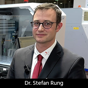
Is it hard to imagine a single laser pulse reduced not only from nanoseconds (0.000000001 s) to picoseconds (0.000000000001 s) in its pulse duration, but even to femtoseconds (0.000000000000001 s)? Well, buckle up because it seems we are there. In this interview, Dr. Stefan Rung, technical director of laser machines at Schmoll Maschinen GmbH, traces the technology trajectory of the laser drill from the CO2 laser to cutting-edge picosecond and hybrid laser drilling systems, highlighting the benefits and limitations of each method, and demonstrating how laser innovations are shaping the future of PCB fabrication.
Marcy LaRont: Stefan, we are here to explore the evolution of laser drilling in PCB fabrication, and what’s new and possible today. Take me through that history and what today’s technology offers the printed circuit board and substrate manufacturer.
Stefan Rung: The laser itself is quite a new tool, relatively speaking. Since its invention in 1960 by Theodore Mayman, there has been a demand for high-throughput tools and lasers. CO2 lasers, with a wavelength in the infrared region at 9.4 µm, were adapted for high-throughput drilling. This was possible because those lasers had the high energy output needed to remove material in a short time.
Additionally, the CO2 laser benefited the PCB industry because it could stop at the copper plane. CO2 lasers have high copper reflectivity, absorption of just a few percentage points. The target copper plane reflects all the light from drilling the organic material, so you have a natural process stop making the CO2 laser process inherently controllable. In mechanical drilling, the longer you drill, the deeper the hole. There is no precise automatic stop that would compensate variations in the layer thickness. For multilayer buildups, using a CO2 laser allowed for lower copper weights on the inner layers. You now had a reliable tool to stop on the copper and create the microvia. This contributed to the broader adoption of the CO2 laser in PCB shops.
As laser technology developed, UV nanosecond lasers emerged. Instead of microsecond-long pulses, they now had hundreds of thousands of nanosecond-long pulses in a typical wavelength of 355 nanometers. These UV lasers showed good absorption of the organic material and copper, allowing us to drill through the copper surface and the organic material.
However, that created a challenge to stop on thin target copper plane. With the more precise laser sources in development over the past decades, it has been easier for process engineers to develop processes to stop when they need to stop. There were also some advantages with specially designed prepreg structures that helped make this process more reliable.
Both rising laser technologies have had their benefits and drawbacks. Now, with hybrid drilling technology, the UV nanosecond laser can penetrate the top copper layer, and then use the microsecond-long pulse CO2 laser to penetrate or to remove the dielectric, which then stops at the next copper plane.
To continue reading this interview, which originally appeared in the June 2025 issue of PCB007 Magazine, click here.


