


 Driving Innovation: Depth Routing Processes—Achieving Unparalleled Precision in Complex PCBs
 It's Only Common Sense: The Evolution of Prospecting
 Dan's Biz Bookshelf: 'Apple in China: The Capture of the World’s Greatest Company'


Real Time with... IPC APEX EXPO 2025: Emerging Trends in Design and Technology
April 16, 2025 | Real Time with...IPC APEX EXPOEstimated reading time: Less than a minute
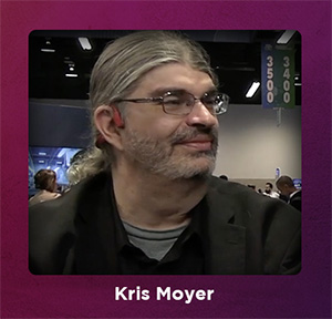
Andy Shaughnessy speaks with IPC design instructor Kris Moyer to discuss emerging design trends. They cover UHDI technology, 3D printing, and optical data transmission, emphasizing the importance of a skilled workforce. The role of AI in design is highlighted, along with the need for understanding physics and mechanics as designs become more complex. The conversation concludes with a focus on enhancing math skills for better signal integrity.
The 25th IPC APEX EXPO, March 18-20, 2025, at the Anaheim Convention Center in California, has concluded successfully. If you couldn’t make it to the show, don’t worry—the I-Connect007 team has coverage of the entire week’s events. Don’t miss our Real Time with… IPC APEX EXPO 2025 video interviews with the movers and shakers of the electronics industry.
Share on:


Testimonial
"In a year when every marketing dollar mattered, I chose to keep I-Connect007 in our 2025 plan. Their commitment to high-quality, insightful content aligns with Koh Young’s values and helps readers navigate a changing industry. "
Brent Fischthal - Koh YoungSuggested Items
The Signal Integrity Issue: Design007 Magazine September 2025
09/09/2025 | I-Connect007 Editorial TeamAs the saying goes, “If you don’t have signal integrity problems now, you will eventually.” This month, our experts share a variety of design techniques that can help PCB designers and design engineers achieve signal integrity.
ASC Sunstone Circuits to Exhibit at AEMS 2025
09/09/2025 | American Standard CircuitsASC Sunstone Circuits will be exhibiting at AEMS 2025 (Anaheim Electronics and Manufacturing Show) to be held at the Anaheim Convention Center on September 24 and 25, 2025.
Automation Meets Sustainability
09/08/2025 | Rick Nichols, GreenSource EngineeringGreenSource Engineering (GSE) is proud to have contributed to the first successful reshoring of a PCB facility on a greenfield site in the United States. While we are honored to have played a key role, full credit for this achievement goes to SEL for its vision, commitment, and professionalism.
Cadence to Acquire Hexagon’s Design & Engineering Business
09/08/2025 | Cadence Design SystemsCadence announced it has entered into a definitive agreement to acquire the Design & Engineering (D&E) business of Hexagon AB, which includes its MSC Software business—a pioneer in engineering simulation and analysis solutions.
Synopsys, GlobalFoundries Establish Pilot Program to Bring Chip Design and Manufacturing to University Classrooms
09/05/2025 | GlobalFoundriesSynopsys, Inc. and GlobalFoundries (GF) announced a new collaboration to launch an educational ‘chip design to tapeout’ program for universities worldwide.