


 American Made Advocacy: Smart Policies Can Ensure AI Data Centers Are Secure
 Beyond the Board: Early Engagement Means Faster Prototyping for Defense Programs
 Defense Speak Interpreted: The Autonomous Plane Battle—Skyborg Vs. Loyal Wingman


PCBAIR Invests in AI to Enhance Defect Prediction in PCB Manufacturing
April 11, 2025 | PRNewswireEstimated reading time: 1 minute
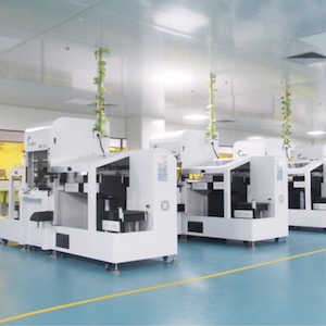
PCBAIR, a leading provider of PCB manufacturing and assembly services with fully automated production lines, announced that it is increasing funding for research and development to incorporate AI into its manufacturing processes, dramatically improving defect prediction accuracy and efficiency.
"We are focused on improving our manufacturing processes," says Dr. Jian Li, Chief Technology Officer at PCBAIR. "Our investment in AI-powered defect prediction represents a major step forward. By applying machine learning and advanced thermal imaging analysis, we can identify potential defects with unprecedented precision, long before they impact product quality."
The core of PCBAIR's research centers on developing sophisticated AI algorithms trained on vast datasets of thermal images and other process data. This allows the system to learn the subtle indicators of potential defects, such as solder joint inconsistencies, component misalignments, and other anomalies that might be missed by traditional inspection methods.
"This technology has the potential to transform how we approach quality control," adds Sarah Chen, Director of Quality Assurance at PCBAIR. "Instead of simply reacting to defects, we can proactively address them, ensuring that every circuit board we produce meets the highest standards of performance and reliability. This is particularly crucial for our customers in demanding sectors like aerospace, medical devices, automotive electronics, and industrial automation, where failure is not an option."
PCBAIR's research also incorporates the integration of AI-driven insights with its existing automated production lines, creating a closed-loop system for continuous improvement. The company anticipates that this technology will not only enhance its own manufacturing capabilities but also provide valuable data for optimizing PCB design and component selection in the future. The aim is making the whole ecosystem from design to manufacture more robust.
Share on:


Testimonial
"Our marketing partnership with I-Connect007 is already delivering. Just a day after our press release went live, we received a direct inquiry about our updated products!"
Rachael Temple - AlltematedSuggested Items
EMS and ODM Market Size to Surpass USD 1589.62 Billion by 2033, Rising at 7.40% CAGR
11/04/2025 | Globe NewswireAccording to the SNS Insider, “The EMS and ODM market size was valued at USD 900.09 Billion in 2025E and is projected to reach USD 1,589.62 Billion by 2033, growing at a CAGR of 7.40% during 2026–2033.”
Electronics Manufacturing Powers U.S. Growth, Supporting 5.2 Million Jobs and $1.8 Trillion in Output
11/03/2025 | Global Electronics AssociationNew report from Global Electronics Association shows electronics industry contributes $853 billion to GDP and delivers average annual wages exceeding $156,000, reinforcing its role as a pillar of U.S. economic resilience.
Nolan’s Notes: Is Mexico the Pulse of Electronics in the Americas?
11/04/2025 | Nolan Johnson -- Column: Nolan's NotesLast year, I attended SMTA Guadalajara, where I saw the results of the Mexican investment in electronics manufacturing. The U.S. was still operating under the Biden administration, and while Mexican EMS companies had expanded capacity to support EV manufacturing, the demand dropped significantly. In my conversations at the show, the sentiment was one of patience. They knew the EV business would likely come back. However, they didn’t expect an overhaul of U.S. trade agreements and tariffs that would shift a more diversified portfolio in Mexico’s direction.
TTM Technologies Receives Two Awards from the Global Electronics Association at the 2025 IPC CEMAC Conference
11/03/2025 | Globe NewswireTTM Technologies, Inc. announced that two of its team members received prestigious Asia Steering Committee Outstanding Service Awards from the Global Electronics Association (formerly named IPC connecting global electronics industry) at the 2025 IPC CEMAC Electronics Manufacturing Annual Conference in Shanghai.
SMT007 Magazine November 2025: Inside Mexico’s Rise as an Electronics Manufacturing Leader
11/04/2025 | I-Connect007 Editorial TeamMexico isn’t just part of the electronics manufacturing conversation—it’s leading it. From growing investments to cross-border collaborations, Mexico is fast becoming the center of electronics in North America. In this issue, we uncover why Mexico is earning global recognition. From top-ranked manufacturing capabilities to expanding partnerships that reach far beyond the U.S.