


 American Made Advocacy: Smart Policies Can Ensure AI Data Centers Are Secure
 Beyond the Board: Early Engagement Means Faster Prototyping for Defense Programs
 Defense Speak Interpreted: The Autonomous Plane Battle—Skyborg Vs. Loyal Wingman


TASMIT Launches Large Glass Substrate Inspection System for Advanced Semiconductor Packaging
March 4, 2025 | ACCESSWIREEstimated reading time: 1 minute
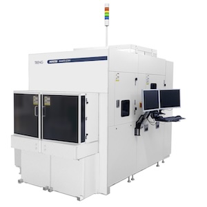
TASMIT Inc. has launched a new inspection system for glass substrates as part of its INSPECTRA® series of semiconductor wafer visual inspection systems, which has gained attention for its high efficiency in advanced semiconductor manufacturing.
The system detects not only pattern defects and foreign particles but also cracks and other defects specific to glass substrates, and is compatible with glass core interposers and rewiring glass carriers, which are used in panel level packaging (PLP) and other applications.
Semiconductor manufacturers have previously introduced inspection systems for detecting surface defects on glass substrates, but this is the industry's first system capable of inspecting both the front and back surfaces as well as the internal structure to date.
TASMIT aims to supply the large glass substrate inspection system to manufacturers of advanced semiconductors, such as PLP, targeting 1 billion yen in orders in FY2025 and 2 billion yen in FY2030.
Currently, in 2.5D packaging, a next-generation semiconductor manufacturing technology, the increasing performance of semiconductors has led to larger semiconductor chips and a higher number of chips per package due to greater integration. As a result, interposers, which serve as intermediate components that electrically connect the chips to the substrate, are also being scaled up.
Traditionally, silicon interposers made from 12-inch silicon wafers have been used, but since wafers are circular, the number of chips that can be produced from a single wafer is limited, making it difficult to meet growing demand. As an alternative, glass substrates are gaining attention as they can be manufactured in large substrate sizes and are suitable for high-density packaging, this new system is compatible with industry-standard 650mm square glass substrates.
However, as glass is prone to microscopic cracks, semiconductors produced using glass substrates may experience operational stability issues, requiring their removal during processing. Traditionally, surface inspection has relied on optical technology, but due to the design of the inspection equipment, only surface defects could be detected, and no equipment could identify backside or internal defects.
Building on the core specifications of the conventional INSPECTRA® series, a new developed glass substrate defect detection and analysis algorithm and an optical inspection mechanism utilizing polarized light have been installed, enabling the industry's first-ever double-sided and internal defect inspection. It also retains the high inspection speed, 40 seconds per panel, of the INSPECTRA® series, which enables 100% inspection and helps prevent defective products from reaching the market.
Share on:


Testimonial
"In a year when every marketing dollar mattered, I chose to keep I-Connect007 in our 2025 plan. Their commitment to high-quality, insightful content aligns with Koh Young’s values and helps readers navigate a changing industry. "
Brent Fischthal - Koh YoungSuggested Items
LPKF Delivers Key Strategic Technology to Fraunhofer's Glass Panel Technology Group
10/29/2025 | LPKFLPKF Laser & Electronics SE is one of the initiators of the Glass Panel Technology Group (GPTG), a consortium encompassing the entire process chain for advanced semiconductor packaging with glass substrates.
Is Glass Finally Coming of Age?
10/13/2025 | Nolan Johnson, I-Connect007Substrates, by definition, form the base of all electronic devices. Whether discussing silicon wafers for semiconductors, glass-and-epoxy materials in printed circuits, or the base of choice for interposers, all these materials function as substrates. While other substrates have come and gone, silicon and FR-4 have remained the de facto standards for the industry.
The Chemical Connection: Experience and Wisdom Gained by Doing Business
09/03/2025 | Don Ball -- Column: The Chemical ConnectionA well-managed company learns to adjust its strategies and processes based on what it learns during challenging times. The experience gained from making (or losing) a difficult sale is invaluable in adapting new sales and manufacturing processes necessary to make that sale the next time, no matter how painful those new processes might be.
Materials and Manufacturing for the AI Era: The Next PCB Frontier
08/08/2025 | Edy Yu, Chief Editor, ECIO, and the I-Connect007 Editorial TeamAI is pushing hardware to its limits, and the bottleneck isn’t design anymore—it’s materials. Next-generation AI servers aren’t just heavier on layer counts. They demand better materials to handle the speed, heat, and signal integrity requirements of 400G, 800G, and even 1.6T Ethernet systems. Many server motherboards are already 32–36 layers. For the next wave of 1.6T-capable boards, expect 40–50 layers, which must maintain high-frequency performance without degrading signal quality.
I-Connect007 Editor’s Choice: Five Must-Reads for the Week
06/27/2025 | Nolan Johnson, I-Connect007While news outside our industry keeps our attention occupied, the big news inside the industry is the rechristening of IPC as the Global Electronics Association. My must-reads begins with Marcy LaRont’s exclusive and informative interview with Dr. John Mitchell, president and CEO of the Global Electronics Association. For designers, have we finally reached the point in time where autorouters will fulfill their potential?