-

- News
- Books
Featured Books
- smt007 Magazine
Latest Issues
Current Issue
Technical Resources
Key industry organizations–all with knowledge sharing as a part of their mission–share their technical repositories in this issue of SMT007 Magazine. Where can you find information critical to your work? Odds are, right here.

The Path Ahead
What are you paying the most attention to as we enter 2025? Find out what we learned when we asked that question. Join us as we explore five main themes in the new year.

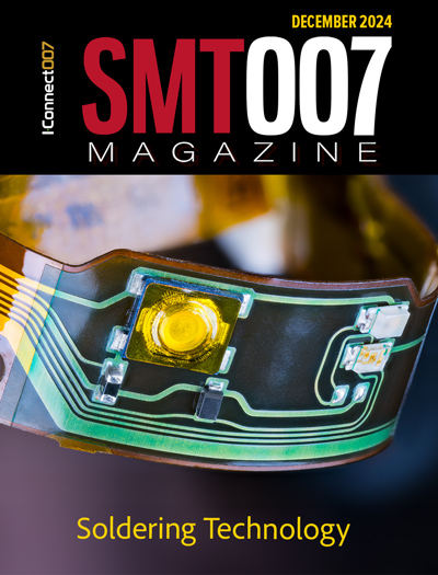
Soldering Technologies
Soldering is the heartbeat of assembly, and new developments are taking place to match the rest of the innovation in electronics. There are tried-and-true technologies for soldering. But new challenges in packaging, materials, and sustainability may be putting this key step in flux.
- Articles
- Columns
Search Console
- Links
- Media kit
||| MENU - smt007 Magazine
Estimated reading time: 8 minutes
Global PCB Connections: The Future of HDI PCBs
High-density interconnect (HDI) printed circuit boards (PCBs) transform modern electronics by providing increased functionality, reduced sizes, and enhanced performance in complex designs. They do so by using advanced techniques, such as finer line and space definitions, microvias, and additional board layers. Specialized via structures—namely blind, buried, and stacked vias—offer complex routing while conserving space. This allows for the development of highly compact electronic devices. This article delves into HDI PCB technology, the function and benefits of blind, buried, and stacked vias, and their impact on PCB performance and design.
HDI PCBs have gained prominence because they support increased circuit densities per unit area compared to conventional PCBs. This stems from incorporating smaller via diameters, reduced trace and space widths, and varied interconnects between layers. These features enable more routing options in a smaller area, valuable for applications needing maximum function in limited space. Some common applications of HDI PCBs include smartphones, tablets, wearable devices, automotive electronics, and medical equipment.
The defining characteristic of HDI technology is its emphasis on miniaturization without compromising functionality or performance. By leveraging HDI attributes PCB designers can design boards that meet advanced electronic devices’ complex requirements. However, with this increase in density and complexity comes the challenge of routing multiple signals through limited spaces. This is where specialized vias are essential.
A via is a small, drilled hole in a PCB to create an electrical connection between layers. In traditional PCBs, through-vias connect the top to the bottom layer, passing through all intermediate and inner layers. The through-via-design takes up valuable real estate on each layer, limiting the routing options and design flexibility in high-density applications. HDI PCBs conserve layer space by using blind and buried vias to make the needed connections.
Blind vias connect an outer layer to one or more of the PCB’s inner layers. Unlike traditional through-vias, blind vias do not extend through the board, stopping instead at a specific inner layer. This type of via connects the surface layer to internal circuitry without affecting the opposing surface layer. This allows for additional signal routing. Blind vias may help reduce the overall size of the PCB by maximizing the space within the board’s layers. They are essential for designs with tight space constraints.
Buried vias connect two or more inner layers but do not extend to the outer layers. This configuration allows for hidden connections within the PCB’s internal layers, offering more routing options without affecting the surface layers. Using buried vias, designers can route complex signal paths inside the board, leaving the surface layers free for additional routing, component placement, or other essential connections. In multilayer designs with densely packed routing channels in their internal layers, buried vias are especially valuable.
Blind and buried vias can be flexible, allowing for a higher density of components and more intricate routing while minimizing interference on other layers. They contribute to enhanced board functionality without increasing board size.
Stacked Vias: Maximizing Density and Signal Integrity
As PCB designs become increasingly complex, it’s essential to have more space-saving and efficient routing options. One solution involves vertically aligning multiple vias across layers using stacked vias. This creates a “stacked” configuration. HDI designs, with their added layers for dense circuitry or high-speed signal paths, particularly benefit from stacked vias. Designers can maximize board density by stacking vias without expanding the board's size or altering its physical footprint.
Stacked Vias in Practice
In HDI design, stacked vias comprise microvias—smaller laser-drilled vias aligned on top of each other. This allows for high-density vertical routing, maximizing available board space. Stacked vias also offer greater flexibility in routing signals across multiple layers, which is beneficial in complex designs where high-density interconnections are required.
Advantages of Stacked Vias
Beyond their space-saving benefits, stacked vias improve signal integrity and reduce impedance, which is vital for high-speed or high-frequency applications. Signal integrity describes how accurately electrical signals transmit through the PCB. In high-speed applications, minimizing impedance is essential to avoid signal loss or distortion. By keeping signal paths shorter and more direct through stacked vias, designers can optimize the electrical performance of the board. This is valuable in applications such as telecommunications, computing, and automotive systems.
Benefits of HDI with Blind, Buried, and Stacked Vias
Integrating blind, buried, and stacked vias enhances the functionality and reliability of the PCB. Key advantages include:
- Increased routing density: Using blind and buried vias, more routing channels become available on each layer, allowing for a higher density of connections within the same board area. They allow designers to create more complex and multifunctional devices without increasing the size of the PCB.
- Improved signal integrity: Stacked vias contribute to improved signal integrity by keeping signal paths shorter and reducing impedance. Improved signal integrity is critical in high-speed applications and helps maintain signal quality and minimize issues such as signal reflection or electromagnetic interference.
- Reduced board size: Using internal connections through blind, buried, and stacked vias demonstrates how PCBs can be made smaller without sacrificing complexity or function. This is important in consumer electronics, medical devices, and other compact design applications.
- Enhanced design flexibility: HDI technology, combined with these via structures, allows for greater design flexibility. Designers can use each layer efficiently by placing components and routing signals without the constraints of traditional through-vias.
HDI PCB Applications
HDI PCBs with blind, buried, and stacked vias are invaluable in industries that demand high performance in compact forms. Mobile devices, wearables, and other portable electronics rely heavily on HDI technology for increased functionality in limited spaces. Automotive electronics and medical equipment also benefit from HDI’s enhanced reliability and durability.
In summary, HDI PCB technology with blind, buried, and stacked vias opens new possibilities for creating compact, high-performance, and reliable PCBs. By optimizing space, enhancing signal integrity, and providing greater design flexibility, these design and fabrication techniques are essential in today’s fast-growing electronic industry. They support the development of next-generation devices that are smaller, smarter, and more efficient.
Meanwhile, let’s stay connected.
Jerome Larez is a field application engineer and director of technical sales with CEE PCB.


