


 Global PCB Connections: Rigid-flex and Flexible PCBs—The Backbone of Modern Electronics
 Flexible Thinking: The Key to a Successful Flex Circuit Design Transfer
 Happy’s Tech Talk #29: Bend-to-Install Semi-flex FR-4


Intel to Sell Minority Stake in IMS Nanofabrication Business to TSMC
September 13, 2023 | IntelEstimated reading time: 2 minutes
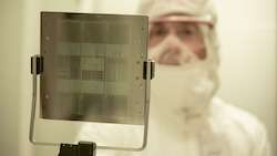
Intel Corporation announced that it has agreed to sell an approximately 10% stake in the IMS Nanofabrication business to TSMC. TSMC’s investment values IMS at approximately $4.3 billion, consistent with the valuation of the recent stake sale to Bain Capital Special Situations. Intel will retain majority ownership of IMS, which will continue to operate as a standalone subsidiary under the leadership of CEO Dr. Elmar Platzgummer. The transaction is expected to close in the fourth quarter of 2023.
IMS is the established industry leader in multi-beam mask writing tools required to develop advanced extreme ultraviolet lithography (EUV), which is broadly adopted in leading-edge technology nodes that enable the most demanding computing applications, such as artificial intelligence (AI) and mobile. Together, Bain Capital and TSMC’s investments provide IMS with increased independence and reinforce confidence in the significant opportunity ahead of IMS. This added autonomy will help IMS accelerate its growth and drive the next phase of lithography technology innovation to enable the industry’s transition into new patterning systems, such as high-numerical-aperture (high-NA) EUV.
Matt Poirier, senior vice president of Corporate Development at Intel, said, “This investment demonstrates the deep industry collaboration IMS is pioneering to advance critical lithography technology for leading-edge nodes, which will benefit the entire semiconductor manufacturing ecosystem. With enhanced independence, IMS will be well positioned to address the significant growth opportunity for multi-beam mask writing tools over the next decade and beyond.”
Platzgummer said, “We are delighted to bring in new investors to help us build on IMS’ leadership in multi-beam mask writing, which is the backbone of innovation in leading-edge semiconductor technologies. This is a testament to IMS’ expertise and leadership position in this integral technology. Together with our partners, we look forward to continuing to support innovation of next-generation technologies and deliver value across the semiconductor ecosystem.”
Dr. Kevin Zhang, senior vice president of Business Development at TSMC, said, “TSMC has been working with IMS since 2012 on the development of multi-beam mask writers for advanced technology nodes. This investment continues the long-term partnership between TSMC and IMS to accelerate innovation and enable deeper cross-industry collaboration.”
IMS plays a critical role in enabling the growth and advancement of the semiconductor industry in an era of ever more demanding applications. Global semiconductor demand continues to grow fueled by five superpowers: AI, pervasive connectivity, ubiquitous computing, cloud-to-edge infrastructure and sensing. The market is expected to reach $1 trillion by 2030. A key enabler of this growth is advances in lithography technology, such as EUV, which is essential for the leading-edge nodes that enable these demanding applications. These lithographic advances rely on sophisticated mask writing tools, which make IMS’ leadership technology central to innovation across the ecosystem.
Intel initially invested in IMS in 2009 and ultimately acquired the remaining stakes in 2015. Since the acquisition, IMS has delivered a significant return on investment to Intel while growing IMS’ workforce and production capacity by four times and delivering three additional product generations. In June 2023, Intel announced an agreement to sell an approximately 20% stake in IMS to Bain Capital.
Share on:


Testimonial
"In a year when every marketing dollar mattered, I chose to keep I-Connect007 in our 2025 plan. Their commitment to high-quality, insightful content aligns with Koh Young’s values and helps readers navigate a changing industry. "
Brent Fischthal - Koh YoungSuggested Items
Circus SE Set for High-Volume Market Entry in the Defense Sector
10/17/2025 | BUSINESS WIRECircus SE a global technology leader in AI robotics for autonomous nutrition systems and troop supply, is expanding its global production network as part of its high-volume market entry into the defense sector.
China Expands Rare Earth Export Restrictions, Tightening Grip on Global Supply Chains
10/16/2025 | I-Connect007 Editorial TeamChina sharply expanded its rare earth export restrictions on Oct. 9, adding additional elements and refining technologies to its control list while imposing stricter rules on foreign users in the defense and semiconductor industries.
SAMI Advanced Electronics Company Launches “Remal” Computer Manufacturing Project in Partnership with HP and Foxconn
10/15/2025 | SAMI-AECSAMI Advanced Electronics Company (SAMI-AEC), a wholly owned subsidiary of Saudi Arabian Military Industries (SAMI), proudly announced the launch of the “Remal” project for computer manufacturing, in strategic partnership with HP and Foxconn.
The Right Approach: Electro-Tek—A Williams Family Legacy, Part 1
10/15/2025 | Steve Williams -- Column: The Right ApproachThere is no bronze bust in the lobby or portrait in the conference room of Electro-Tek's founder—my Dad, Charles “Chuck” Williams—so with the facility closing last year after 56 years, I feel it is time to tell the story. Chuck Williams founded Electro-Tek in 1968 in our basement, eventually moving into the second floor of an old 1913 building in downtown Milwaukee that is still standing (the first of three eventual facilities).
LPKF Joins productronica’s 50th Anniversary, Showcasing Laser Technology for Electronics Manufacturing
10/10/2025 | LPKF Laser & ElectronicsLPKF Laser & Electronics invites visitors to productronica 2025 in Munich from November 18 to 21. At booth 305 in hall B2, the company will present its portfolio of modern laser technologies for the electronics industry live – from prototyping systems and high-performance depaneling to laser plastic welding for electronic housings and thin glass processing for advanced packaging.