


 Global PCB Connections: Rigid-flex and Flexible PCBs—The Backbone of Modern Electronics
 Flexible Thinking: The Key to a Successful Flex Circuit Design Transfer
 Happy’s Tech Talk #29: Bend-to-Install Semi-flex FR-4


Lockheed Martin Delivers Initial 5G Testbed To U.S. Marine Corps And Begins Mobile Network Experimentation
September 1, 2023 | Lockheed MartinEstimated reading time: 2 minutes
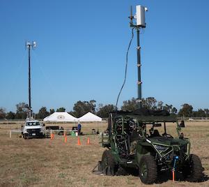
Lockheed Martin delivered the final Phase 1 Initial Prototype 5G testbed variant for the Open Systems Interoperable and Reconfigurable Infrastructure Solution (OSIRIS) to the Marine Corps program management team aboard Marine Corps (USMC) Base Camp Pendleton, California, and will begin mobile network experimentation. OSIRIS is a 5G communications network infrastructure testbed for expeditionary operations experimentation for the Office of the Under Secretary of Defense for Research and Engineering’s (OUSD R&E) FutureG & 5G Office and the USMC that was awarded to Lockheed Martin in 2021.
Phase 2, experimentation, continues Lockheed Martin’s partnership with the USMC to integrate specific mission applications onto the OSIRIS 5G testbed for evaluation. In parallel, emerging wireless technology will be assessed and selected for use as part of the continued build out of the OSIRIS 5G testbed concluding with three distinct 5G standalone network configurations:
- Trailer-mounted 5G Nomadic Tower
- ATV-mounted 5G Mobile Relay
- Transit case deployable 5G Operational Facility
“The Lockheed Martin-led team, in close partnership with the U.S. Marine Corps has proven that quickly evolving 5G commercial technology can be leveraged in near real-time to solve current and emergent mission challenges,” said Deon Viergutz, vice president, Lockheed Martin Spectrum Convergence. “The OSIRIS program is leveraging Lockheed Martin’s experience maturing vendor-interoperable solutions based on open standards, which will enable a wide variety of composable 5G solutions tailored to any mission and platform.”
The Lockheed Martin-led team, with subcontractors Intel Corporation (Nasdaq: INTC), Radisys Corporation (NASDAQ: RSYS) and Rampart Communications, Inc., has worked closely with the PM team aboard Camp Pendleton, and the team will continue their close collaboration with the USMC and OUSD R&E over the next 15 months to test, evaluate and ultimately demonstrate the technology as part of a Fleet Marine Force (FMF) event in the Southern California region.
Increased Bandwidth, Faster Speeds in Minutes Instead of Hours
To progress from phase 1 to the experimentation phase, the team successfully integrated an Open Radio Unit (O-RU) with Lockheed Martin’s hybrid base station running Intel's FlexRAN reference software and hardware technology including Intel Xeon processors, ethernet adapters and accelerators. This integration makes the OSIRIS system one of the first tactical 5G standalone small cell systems compliant with the Open-Radio Access Network (O-RAN) 7.2 split architecture.
O-RAN 7.2 split architecture compliance optimizes the OSIRIS system to oversee increases in bandwidth while also maximizing virtualization of shared resources like radios.
This is crucial to supporting the USMC’s Expeditionary Advanced Base Operations (EABO) goals, which involve Marines operating in contested environments with increased bandwidth requirements. Additionally, the OSIRIS system aims to reduce overall set-up time.
OSIRIS, a key initiative of Lockheed Martin’s 5G.MIL® programs, will help address the need for test facilities that enable rapid experimentation and dual-use application prototyping. Here is how:
- The testbed will identify areas for further synergy between 5G networks and DOD platforms that will enhance customer capabilities.
- The infrastructure will allow for the connection of various 5G-ready user devices, sensors, vehicles, and endpoints to explore the military utility of commercial 5G technologies and pave the way for onboarding of new technologies from other OUSD investments while simultaneously addressing cybersecurity requirements.
- This capability will further enable and advance DOD’s Joint All Domain Operations concept.
Share on:


Testimonial
"We’re proud to call I-Connect007 a trusted partner. Their innovative approach and industry insight made our podcast collaboration a success by connecting us with the right audience and delivering real results."
Julia McCaffrey - NCAB GroupSuggested Items
Microchip Enters into Partnership Agreement with Delta Electronics on Silicon Carbide Solutions
07/18/2025 | Globe NewswireThe growth of artificial intelligence (AI) and the electrification of everything are driving an ever-increasing demand for higher levels of power efficiency and reliability.
ViTrox’s HITS 5.0 Empowers Global Partners with Innovative Solutions and Stronger Bonds
07/16/2025 | ViTroxViTrox, strives to be the World’s Most Trusted Technology Company, proudly announces the successful conclusion of its fifth edition of High Impact Training for Sales (HITS 5.0), held from 23rd to 27th June 2025 at ViTrox Campus 2.0 and 3.0, located in Batu Kawan Industrial Park, Penang, Malaysia.
Global Citizenship: The Global Push for Digital Inclusion
07/16/2025 | Tom Yang -- Column: Global CitizenshipIt can be too easy to take the technology at our fingertips for granted: high-speed internet, cloud-based collaboration, and instant video calls across continents. Yet, for billions of people, access to these digital tools is a distant dream. As a global community, we must ensure that technology is available to all. Here is how technology is bridging physical, economic, and educational gaps in underserved regions and profoundly reshaping lives.
Microchip Expands Space-Qualified FPGA Portfolio with New RT PolarFire® Device Qualifications and SoC Availability
07/10/2025 | MicrochipContinuing to support the evolving needs of space system developers, Microchip Technology has announced two new milestones for its Radiation-Tolerant (RT) PolarFire® technology: MIL-STD-883 Class B and QML Class Q qualification of the RT PolarFire RTPF500ZT FPGA and availability of engineering samples for the RT PolarFire System-on-Chip (SoC) FPGA.
Infineon Advances on 300-millimeter GaN Manufacturing Roadmap as Leading Integrated Device Manufacturer (IDM)
07/10/2025 | InfineonAs the demand for gallium nitride (GaN) semiconductors continues to grow, Infineon Technologies AG is poised to capitalize on this trend and solidify its position as a leading Integrated Device Manufacturer (IDM) in the GaN market.