


 Beyond the Board: How a Diminished Supplier Base Affects Complex PCB Manufacturing Readiness in Defense
 Defense Speak Interpreted: Hypersonics Report Back After Six Years of Silence
 American Made Advocacy: American Microelectronics Power the Future of High Technology


Thin-Film Tandem Cells Made of Perovskite and Cigse Semiconductors
February 15, 2019 | HZBEstimated reading time: 2 minutes
An HZB team has fabricated and characterized a thin-film tandem solar cell made of perovskite and CIGSe. They relied on a simple, robust fabrication process that is also suitable for scaling up to large surface areas. The tandem solar cell is a fully thin film device with an impressive efficiency of 21.6%. With further improvements it might reach efficiencies above 30%.
Tandem solar cells consist of two semiconductors with different band gaps, enabling them to use a larger fraction of the solar spectrum for generating electricity. This concept is particularly successful when conventional absorber layers such as silicon or copper indium gallium selenide (CIGSe) are combined with the new metal-halide semiconductor perovskite. This is because perovskites convert the blue, high-energy portions of sunlight into electrical energy very efficiently, while silicon or CIGSe convert the red and near-infrared portions effectively.
CIGSe and Perovskite Thin Films Combined
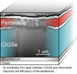
HZB researchers have now combined a thin-film solar cell made of CIGSe with a thin layer of perovskite. The CIGSe thin film was grown on a substrate, resulting in a CIGSe surface that is typically rough and irregular. This has made the application of the perovskite top cell using wet-chemical methods more difficult thus far.
Ultrathin Layer Improves Cell Efficiency
The HZB team in cooperation with Eindhoven University of Technology has now for the first time improved the properties of the tandem solar cell by applying an ultra-thin yet conformal intermediate layer to the CIGSe layer, then spin-coating the perovskite layer onto it at the HySPRINT lab of HZB. The tandem solar cell produced in this way converts 21.6% of the solar spectrum into electrical energy. This power conversion efficiency remains stable.
Manufacture Requires Minimal Energy
Although tandem cells made of silicon and perovskite achieve even higher efficiencies so far, theoretically, CIGSe perovskite tandem cells could also achieve these efficiencies. In addition, the new CIGSe perovskite tandem cell is a fully thin film device. This means that the new tandem cell is made from thin layers of CIGSe and perovskite so that the material and energy consumed during its manufacture are extremely low.
Mass Production Feasible
“This tandem cell was fabricated on a rough, untreated CIGS bottom cell, which simplifies manufacture and represents an enormous advantage in terms of mass production“, Prof. Dr. Rutger Schlatmann, Director of the HZB Institute PVcomB, points out.
The tandem solar cell was realised on an area of 0.8 square centimetres, which is considerably larger than the square-millimetre areas commonly used in laboratory research.
“Record values are only recognised for areas of one square centimetre or more, yet our cell area is just slightly below this threshold. Therefore, we now focus to certify this tandem solar cell efficiency and its enormous performance by an independent institution“, says Prof. Dr. Steve Albrecht, head of a Young Investigator Group at HZB, funded by the Federal Ministry for Education and Research (BMBF).
Outlook: Possible Efficiencies of Over 30%
Using electron microscopy and other measurements, first author Dr. Marko Jost, a postdoc in Steve Albrecht's team, and his colleagues analysed the conformal layer structure of the tandem cell and were also able to determine the contributions of the individual sub-cells to the performance of the tandem cell. Their study points out ways to further improve monolithic perovskite/CIGSe tandem cells and achieve efficiencies of over 30%.
Share on:


Testimonial
"In a year when every marketing dollar mattered, I chose to keep I-Connect007 in our 2025 plan. Their commitment to high-quality, insightful content aligns with Koh Young’s values and helps readers navigate a changing industry. "
Brent Fischthal - Koh YoungSuggested Items
Nortech Systems Launches Power over Fiber Technology Platform for EMI-Sensitive Applications
04/08/2026 | Globe NewswireNortech Systems Incorporated, a leading provider of design and manufacturing solutions for complex electromedical devices and electromechanical systems, has announced the launch of its Power over Fiber technology platform.
Flexible Thinking: Designing Flex Circuits for Dynamic Reliability
04/09/2026 | Joe Fjelstad -- Column: Flexible ThinkingFlex circuits flex. No surprises there. However, they are also very commonly designed into products because they are thin and offer consistent thickness and dielectric properties, attributes highly prized by present-day product designers of personal electronics. This would include smartphones and, increasingly, wearable electronics for medical monitoring and even fashion.
Understanding Tolerances in Flexible Circuit Design
04/01/2026 | Chris Clark, Flexible Circuit TechnologiesThe challenge with cumulative tolerances is meeting the dimensional requirements for items dimensioned on a drawing or specification for a flexible or rigid-flex circuit. It is critical to understand the fabrication processes and how features are defined when creating your tolerance requirements.
Target Condition: An Exploration of Flooding PCB Layers
04/02/2026 | Kelly Dack -- Column: Target ConditionThe concept of flooding PCB layers with copper has been around for so long, you’d think we’d have it mastered. We haven’t. (Oh, and by “we,” I mean design engineers and the software tools we depend on.) Years ago, PCB artwork was created by hand using light tables, with tape applied to Mylar. Signals were slow, traces were relatively wide, and high-current paths were simply “beefed up” with wider copper. Signal integrity wasn’t yet a driving concern. Today, solid return paths are fundamental to robust design. We understand the importance of continuous reference planes for signal integrity and EMI control.
New, Greener Solutions for Etch: Novel Copper Extraction
03/30/2026 | Richard Nichols, GreenSource Engineering“Novel” is a typical marketing phrase that implies new and unique, but often “novel” actually means an established technology being applied to a new field or application. This, in turn, is often driven by newly relevant external motivation. GreenSource has been working on just such a solution: novel copper extraction, offering a better and greener alternative to traditional LLE control systems for cupric chloride etch.