


 SMT Perspectives & Prospects: The Architecture of Winston Churchill’s Leadership
 Global Sourcing Spotlight: Making Global Sourcing Simple Again
 The Government Circuit: New Council Now Helps Shape Policy Decisions in the Electronics Supply Chain


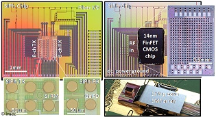
Imec, the world-leading research and innovation hub in nano-electronics and digital technology, announced that it has demonstrated ultra-low power, high-bandwidth optical transceivers through hybrid integration of Silicon Photonics and FinFET CMOS technologies. With a dynamic power consumption of only 230fJ/bit and a footprint of just 0.025mm2, the 40Gb/s non-return-to-zero optical transceivers mark an important milestone in realizing ultra-dense, multi-Tb/s optical I/O solutions for next-generation high-performance computing applications.
The exponentially growing demand for I/O bandwidth in datacenter switches and high-performance computing nodes is driving the need for tight co-integration of optical interconnects with advanced CMOS logic, covering a wide range of interconnect distances (1m-500m+). In the presented work, a differential FinFET driver was co-designed with a Silicon Photonics ring modulator, and achieved 40Gb/s NRZ optical modulation at 154fJ/bit dynamic power consumption. The receiver included a FinFET trans-impedance amplifier (TIA) optimized for operation with a Ge waveguide photodiode, enabling 40Gb/s NRZ photodetection with an estimated sensitivity of -10dBm at 75fJ/bit power consumption. High-quality data transmission and reception was also demonstrated in a loop-back experiment at 1330nm wavelength over standard single mode fiber (SMF) with 2dB link margin. Finally, a 4x40Gb/s, 0.1mm2 wavelength-division multiplexing (WDM) transmitter with integrated thermal control was demonstrated, enabling bandwidth scaling beyond 100Gb/s per fiber.
“The demonstrated hybrid FinFET-Silicon Photonics platform integrates high-performance 14nm FinFET CMOS circuits with imec’s 300mm Silicon Photonics technology through dense, low-capacitance Cu micro-bumps. Careful co-design in this combined platform has enabled us to demonstrate 40Gb/s NRZ optical transceivers with extremely low power consumption and high bandwidth density,” says Joris Van Campenhout, director of the Optical I/O R&D program at imec. “Through design optimizations, we expect to further improve the single-channel data rates to 56Gb/s NRZ. Combined with wavelength-division multiplexing, these transceivers provide a scaling path to ultra-compact, multi-Tb/s optical interconnects, which are essential for next-generation high-performance systems.”
This work has been carried out as part of imec’s industrial affiliation R&D program on Optical I/O and was presented at the 2018 Symposia on VLSI Technology and Circuits (June 2018) in a “late news” paper. Imec’s 200mm and 300mm Silicon Photonics technologies are available for evaluation by companies and academia through imec’s prototyping service and the iSiPP50G multi-project wafer (MPW) service.
About imec
Imec is the world-leading research and innovation hub in nanoelectronics and digital technologies. The combination of our widely acclaimed leadership in microchip technology and profound software and ICT expertise is what makes us unique. By leveraging our world-class infrastructure and local and global ecosystem of partners across a multitude of industries, we create groundbreaking innovation in application domains such as healthcare, smart cities and mobility, logistics and manufacturing, energy and education.
As a trusted partner for companies, start-ups and universities we bring together close to 4,000 brilliant minds from over 85 nationalities. Imec is headquartered in Leuven, Belgium and has distributed R&D groups at a number of Flemish universities, in the Netherlands, Taiwan, USA, China, and offices in India and Japan. In 2017, imec's revenue (P&L) totaled 546 million euro. Further information on imec can be found here.


