-

- News
- Books
Featured Books
- smt007 Magazine
Latest Issues
Current Issue
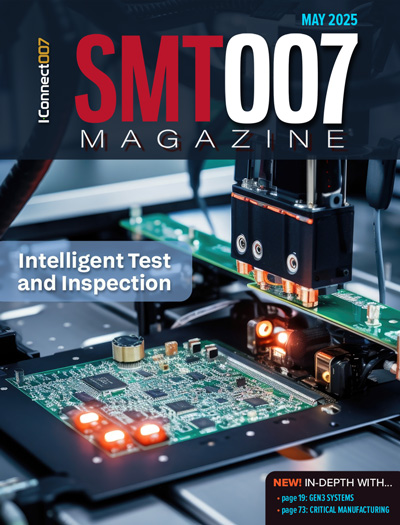
Moving Forward With Confidence
In this issue, we focus on sales and quoting, workforce training, new IPC leadership in the U.S. and Canada, the effects of tariffs, CFX standards, and much more—all designed to provide perspective as you move through the cloud bank of today's shifting economic market.

Intelligent Test and Inspection
Are you ready to explore the cutting-edge advancements shaping the electronics manufacturing industry? The May 2025 issue of SMT007 Magazine is packed with insights, innovations, and expert perspectives that you won’t want to miss.

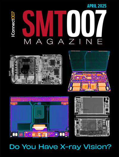
Do You Have X-ray Vision?
Has X-ray’s time finally come in electronics manufacturing? Join us in this issue of SMT007 Magazine, where we answer this question and others to bring more efficiency to your bottom line.
- Articles
- Columns
- Links
- Media kit
||| MENU - smt007 Magazine
RF PCB Design Tips and Tricks
May 8, 2025 | Cherie Litson, EPTAC MIT CID/CID+Estimated reading time: 1 minute
There are many great books, videos, and information online about designing PCBs for RF circuits. A few of my favorite RF sources are Hans Rosenberg, Stephen Chavez, and Rick Hartley, but there are many more. These PCB design engineers have a very good perspective on what it takes to take an RF design from schematic concept to PCB layout.
Here’s a quick summary of the common suggestions that I’ve learned from them and others over time:
- A schematic shows the “ideal” functionality of the RF circuit. When creating a schematic in the PCB layout, the “real” physics of the copper strips, dielectric material, and adjacent circuits and metal features create parasitic influences: resistance, inductance, and capacitance.
- It is the responsibility of the layout engineer to minimize the differences between the “ideal” and “real.”
- Electronic devices and systems operate at frequencies ranging from a few megahertz to several gigahertz. Finding the best method to control the parasitic influences requires only a few basic guidelines.
- Identify and understand the current loops in the circuit
- The shorter the loop, the lower the impedance and resistance ratios
- Use an uninterrupted ground plane as close as possible to the referenced signal
- Give each ground connection its own via as close as possible to the pad
To do this in a PCB, remember it is a 3D environment. Uninterrupted ground plane layers close to their signal, impedance calculations, material selection, copper thicknesses, trace thicknesses, shielding, and spacing become the tools to control the parasitic influences of the “real” circuit.
Methods for applying each of these tools in your PCB design are available for all designers. Then download a tool such as Saturn’s free PCB Toolkit and see how switching to different parameters in the “differential pairs/XTALK” tab will change the values of your target impedances. This will get you in the ballpark of creating a good RF design.
To continue reading this article, which originally appeared in the April 2025 issue of Design007 Magazine, click here.
Suggested Items
PCBA Market to Reach $147.5 Billion by 2035, Growing at a CAGR of 4.7% from 2025
06/27/2025 | PRNewswireThe Printed Circuit Board Assembly market is projected to reach $147.5 billion by 2035, up from an estimated $90.91 billion in 2025, growing at a steady CAGR of 4.7% during the forecast period.
I-Connect007 Editor’s Choice: Five Must-Reads for the Week
06/27/2025 | Nolan Johnson, I-Connect007While news outside our industry keeps our attention occupied, the big news inside the industry is the rechristening of IPC as the Global Electronics Association. My must-reads begins with Marcy LaRont’s exclusive and informative interview with Dr. John Mitchell, president and CEO of the Global Electronics Association. For designers, have we finally reached the point in time where autorouters will fulfill their potential?
Indium Corporation Expert to Present on Automotive and Industrial Solder Bonding Solutions at Global Electronics Association Workshop
06/26/2025 | IndiumIndium Corporation Principal Engineer, Advanced Materials, Andy Mackie, Ph.D., MSc, will deliver a technical presentation on innovative solder bonding solutions for automotive and industrial applications at the Global Electronics A
Summit Interconnect Participates in PCBAA Annual Meeting to Advance U.S. Electronics Policy
06/26/2025 | Summit Interconnect, Inc.Summit Interconnect was proud to participate in the 2025 Annual Meeting of the Printed Circuit Board Association of America (PCBAA), held in Washington, D.C. this June.
DownStream Acquisition Fits Siemens’ ‘Left-Shift’ Model
06/26/2025 | Andy Shaughnessy, I-Connect007I recently spoke to DownStream Technologies founder Joe Clark about the company’s acquisition by Siemens. We were later joined by A.J. Incorvaia, Siemens’ senior VP of electronic board systems. Joe discussed how he, Rick Almeida, and Ken Tepper launched the company in the months after 9/11 and how the acquisition came about. A.J. provides some background on the acquisition and explains why the companies’ tools are complementary.


