-

- News
- Books
Featured Books
- smt007 Magazine
Latest Issues
Current Issue
What's Your Sweet Spot?
Are you in a niche that’s growing or shrinking? Is it time to reassess and refocus? We spotlight companies thriving by redefining or reinforcing their niche. What are their insights?

Moving Forward With Confidence
In this issue, we focus on sales and quoting, workforce training, new IPC leadership in the U.S. and Canada, the effects of tariffs, CFX standards, and much more—all designed to provide perspective as you move through the cloud bank of today's shifting economic market.

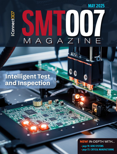
Intelligent Test and Inspection
Are you ready to explore the cutting-edge advancements shaping the electronics manufacturing industry? The May 2025 issue of SMT007 Magazine is packed with insights, innovations, and expert perspectives that you won’t want to miss.
- Articles
- Columns
- Links
- Media kit
||| MENU - smt007 Magazine
OKI Develops 124-Layer PCB Technology for Next-Generation AI Semiconductor Testing Equipment
April 28, 2025 | BUSINESS WIREEstimated reading time: 1 minute
OKI Circuit Technology, the OKI Group printed circuit board (PCB) company, has successfully developed 124-layer PCB technology for wafer inspection equipment designed for next-generation high bandwidth memory, such as HBM mounted on AI semiconductors. This is a roughly 15% increase in the number of layers over conventional 108-layer designs. OTC is seeking to establish mass production technology by October 2025 at its Joetsu Plant in Joetsu City, Niigata Prefecture, which has a proven track record and advanced development and production capabilities in the field of high multilayer, high-precision, large-format PCBs for semiconductor inspection equipment.
AI processing requires the transmission of vast data volumes between graphics processing unit (GPU) semiconductors and memory. As semiconductor performance increases, the memory installed is also required to have high-speed, high-frequency, and high-density data transfer capabilities. HBM features a stacked DRAM structure, requiring technology capable of fabricating wafers even more thinly and precisely. This configuration also requires that the PCBs used in inspection equipment meet even higher levels of performance and quality.
Since the latest semiconductors process an enormous number of signals and the number of wafer-mounted chips increases due to process miniaturization, it is necessary to increase density and more layers on the PCBs used in inspection equipment. Nevertheless, PCB thickness has been limited to 7.6 mm due to various constraints, and 108 layers was the maximum limit with conventional technology. This time, by developing ultra-thin materials and tools and handling technologies suitable for ultra-thin materials, together with developing and introducing a proprietary automatic transport system for ultra-thin materials into its production line, OTC has successfully developed 124-layer PCB technology with a board thickness of 7.6 mm.
OKI is actively engaged in its EMS business based on the core idea of providing comprehensive manufacturing services from design to production and reliability testing. OKI places a particular focus on technology development in the PCB business, and this new technology was developed in response specifically to the areas expected to show future growth, including AI semiconductors, aerospace, defense, robotics, and next-generation communications. OKI will continue to develop PCBs and manufacturing technologies to respond to future progress in technology.
OTC will exhibit at the OTC booth (No.305) at PCB East 2025, which will be held at the Boxboro Regency Hotel and Conference Center in Massachusetts, USA from April 30 to May 2, 2025, to introduce this technology.
Testimonial
"The I-Connect007 team is outstanding—kind, responsive, and a true marketing partner. Their design team created fresh, eye-catching ads, and their editorial support polished our content to let our brand shine. Thank you all! "
Sweeney Ng - CEE PCBSuggested Items
Federal Electronics Mexico Boosts Speed and Flexibility with New Mycronic A40DX Pick-and-Place
07/23/2025 | Federal ElectronicsFederal Electronics, a leader in providing advanced electronic manufacturing services, has announced a major upgrade at its Hermosillo, Mexico facility with the installation of a Mycronic MYPro A40DX Pick-and-Place system, advancing its surface mount assembly capabilities for high-reliability electronics manufacturing.
DuPont Publishes 2025 Sustainability Report
07/22/2025 | PRNewswireDuPont published its 2025 Sustainability Report detailing the progress made toward achieving its 2030 Sustainability Goals.
NEOTech’s Westborough Facility Achieves AS9100 Surveillance Audit, Reinforcing Trust with Aerospace & Defense Customers
07/22/2025 | NEOTechNEOTech, a premier provider of electronic manufacturing services (EMS), integrated design engineering, and advanced supply chain solutions for the aerospace and defense, medical device, and high-tech industrial markets, proudly announces that its Westborough, Massachusetts facility has successfully completed the rigorous AS9100 Bi-Annual Surveillance Audit with zero findings, a testament to the company’s unwavering commitment to quality, security, and operational excellence.
PCBAA Wins Summit Silver Award from the American Society of Association Executives
07/18/2025 | PCBAAPCBAA was one of 38 associations that earned Silver Awards for outstanding contributions for an entry titled: Chips Don’t Float: More Printed Circuit Boards Must be Made in America.
INSPECTIS AB ‘Makes it a Meal’ with Series U50s Advanced Kit
07/18/2025 | INSPECTIS ABFamous chefs the world over maintain that an entrée doesn’t make a great meal without side dishes. At INSPECTIS, we call those ‘sides’ an Advanced Kit.


