-

- News
- Books
Featured Books
- smt007 Magazine
Latest Issues
Current Issue
The Path Ahead
What are you paying the most attention to as we enter 2025? Find out what we learned when we asked that question. Join us as we explore five main themes in the new year.

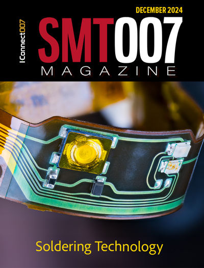
Soldering Technologies
Soldering is the heartbeat of assembly, and new developments are taking place to match the rest of the innovation in electronics. There are tried-and-true technologies for soldering. But new challenges in packaging, materials, and sustainability may be putting this key step in flux.

The Rise of Data
Analytics is a given in this industry, but the threshold is changing. If you think you're too small to invest in analytics, you may need to reconsider. So how do you do analytics better? What are the new tools, and how do you get started?
- Articles
- Columns
Search Console
- Links
- Media kit
||| MENU - smt007 Magazine
NAMICS Brings Innovative Thermoset Materials to PCB Fabrication
January 16, 2025 | Andy Shaughnessy, Design007 MagazineEstimated reading time: 1 minute
At PCB Carolina, Matt Lake and Ken Araujo of NAMICS Technologies spoke with Andy Shaughnessy about the introduction of an innovative thermoset material to PCB fabrication. This groundbreaking material, originally developed for the semiconductor packaging industry, addresses a longstanding demand for unreinforced thermoset films that enhance dielectric properties in PCB applications and allow for manufacturing the very finest of features, 0.002" and below. With its ability to integrate seamlessly into existing processes and equipment, this promises to meet the evolving needs of fabricators, particularly in UHDI and high-frequency products.
Andy Shaughnessy: Matt and Ken, you have a material that's actually been used in the packaging world for quite some time, but you are now introducing it into PCB fabrication. Is this addressing a long-time need?
Matt Lake: I've been in this industry for the better part of 42 years as either a laminate or board manufacturer. At least once a month, a board supplier has said to me, “Can you supply us with your resin simply cast onto a film for applications where we need to fill heavy coppers not necessarily for via fill?”
NAMICS has been making this material for a long time but for a different industry. Traditionally, films that are thermoplastics just don’t work well in these applications. The NAMICS product is a thermoset material. The range of thicknesses fits perfectly into the PCB market. It's been very well received, and enough to keep me from fully retiring.
Shaughnessy: Ken, what are the specifics of this thermoset material, and how was it originally developed for the semiconductor packaging industry?
Ken Araujo: We developed this film called ADFLEMA (Advanced Flexible Materials) well over 15 years ago. The idea was to develop a very low-loss A-stage thermoset film that can be used in developing build-up layers in advanced packaging, commonly on the wafer level.
To continue reading this interview, which originally published in the December 2024 issue of PCB007 Magazine, click here.
Suggested Items
U.S. Department of Commerce Announces $1.4 Billion in Final Awards to Support the Next Generation of U.S. Semiconductor Advanced Packaging
01/17/2025 | U.S. Department of CommerceThe U.S. Department of Commerce has announced that CHIPS National Advanced Packaging Manufacturing Program (NAPMP) has finalized $1.4 billion in award funding to bolster U.S. leadership in advanced packaging and enable new technologies to be validated and transitioned at scale to U.S. manufacturing.
Spirit Announces Sale of FMI to Tex Tech Industries
01/14/2025 | Spirit AeroSystems Holdings, Inc.Spirit AeroSystems Holdings, Inc. announced the sale of Fiber Materials Inc (FMI) business based in Biddeford, Maine, and Woonsocket, Rhode Island, to Tex Tech Industries, Inc. (Tex-Tech) for $165 million in cash.
Imec Achieves Breakthrough in Silicon Photonics
01/13/2025 | ImecImec, a world-leading research and innovation hub in nanoelectronics and digital technologies, has announced a significant milestone in silicon photonics with the successful demonstration of electrically-driven GaAs-based multi-quantum-well nano-ridge laser diodes fully, monolithically fabricated on 300 mm silicon wafers in its CMOS pilot prototyping line.
SolderKing to Highlight Innovations in Soldering and Manufacturing Efficiency at Southern Manufacturing & Electronics 2025
01/08/2025 | SolderKing Assembly Materials Ltd,SolderKing, a leading UK manufacturer of advanced soldering materials and consumables, will be exhibiting at the Southern Manufacturing and Electronics Show from 4-6 February 2025 at the Farnborough International Exhibition Centre, Stand J90.
SMTA Announces Wafer-Level Packaging Symposium Program
01/08/2025 | SMTAThe SMTA is excited to announce the technical program for the 2025 Wafer-Level Packaging Symposium. The symposium will be held February 18-20, 2025 at The Hyatt Regency San Francisco Airport in San Francisco, California.


