-

- News
- Books
Featured Books
- smt007 Magazine
Latest Issues
Current Issue
The Rise of Data
Analytics is a given in this industry, but the threshold is changing. If you think you're too small to invest in analytics, you may need to reconsider. So how do you do analytics better? What are the new tools, and how do you get started?

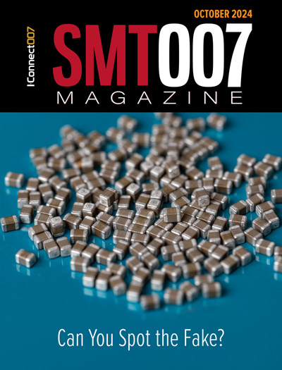
Counterfeit Concerns
The distribution of counterfeit parts has become much more sophisticated in the past decade, and there's no reason to believe that trend is going to be stopping any time soon. What might crop up in the near future?

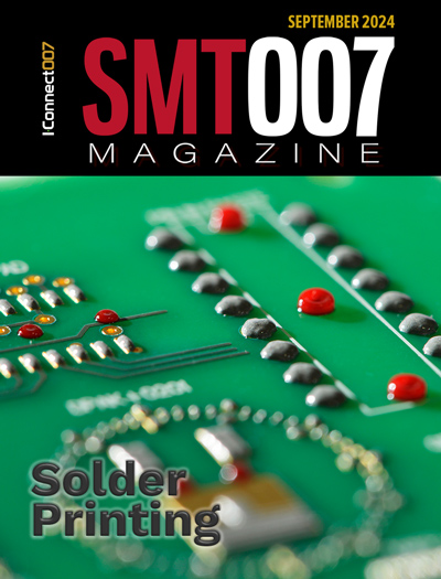
Solder Printing
In this issue, we turn a discerning eye to solder paste printing. As apertures shrink, and the requirement for multiple thicknesses of paste on the same board becomes more commonplace, consistently and accurately applying paste becomes ever more challenging.
- Articles
- Columns
Search Console
- Links
- Media kit
||| MENU - smt007 Magazine
Cadence Unveils Arm-Based System Chiplet
November 20, 2024 | Cadence Design SystemsEstimated reading time: 2 minutes
Cadence has announced a groundbreaking achievement with the development and successful tapeout of its first Arm-based system chiplet. This innovation marks a pivotal advancement in chiplet technology, showcasing Cadence's commitment to driving industry-leading solutions through its chiplet architecture and framework.
The First System Chiplet
In a significant leap forward, Cadence has successfully prototyped, designed, and taped out the industry's first system chiplet. This chiplet integrates processors, system IP, and memory IP within a single package, interconnected through the Universal Chiplet Interconnect Express™(UCIe™) standard interface. Developed with Arm, the chiplet complies with Arm's Chiplet System Architecture (CSA), a standard that ensures interoperability and speeds time-to-market for chiplets.
A system chiplet includes functionality to manage the resources and functionality of the overall multi-chiplet SoC. Featuring components such as a system processor, safety management processor, Cadence controllers, and Cadence PHY IP for LPDDR5 and UCIe, the chiplet is a testament to Cadence's innovation. Using Cadence Janus NoC technology, the chiplet accommodates up to 64GB/s peak bandwidth for UCIe IP and 32GB/s peak memory bandwidth for LPDDR5 IP.
Advancing the Chiplet Ecosystem with Arm
In March 2024, Cadence and Arm formalized their longstanding collaboration to deliver a chiplet-based reference design and a cutting-edge software development platform. This partnership combines Cadence's robust IP and EDA solutions with Arm's state-of-the-art IP technologies, significantly reducing design complexity and accelerating time-to-market for customers. The alliance sets the stage for further advancements, offering customers a comprehensive development platform for unprecedented performance and efficiency.
The central strategy for this collaboration is investing in the Arm CSA, enabling greater component reuse between suppliers. Cadence is an active contributor to the CSA and is developing chiplets that comply with this standard. These standards allow scale and faster time-to-market for chiplets, including Arm Compute Subsystems (CSS) and the Cadence system chiplet.
Advanced IP Technology Innovations
Capitalizing on decades of expertise in IP and subsystem design, the Silicon Solutions Group delivers high-value solutions that address customer challenges. Abstracting functionality into chiplet IP empowers customers to bring innovations to market more quickly. Cadence's mastery of advanced packaging and interconnect technologies enables scalable, high-performance solutions that enhance efficiency and drive technological progress.
Transforming Industries with Chiplet Technology
The shift from monolithic SoCs to chiplet-based designs is driven by the need for enhanced design efficiency, faster platform refresh cycles, and optimized power, performance, and area (PPA) metrics. Chiplets enable a multi-foundry business model, integrating cross-foundry process technologies within the same package. As technology density scaling slows, chiplets become essential in overcoming Moore's Law limits and process reticle constraints. New packaging and interconnect solutions, including 2.5D and 3D packaging and die-to-die interfaces like UCIe, support this transformative approach, offering customers a path to accelerated innovation and market readiness.
Conclusion
Cadence's pioneering work in chiplet technology represents a significant advance in the semiconductor industry. Cadence is setting new benchmarks for efficiency, scalability, and performance through innovative architectures, robust IP, and strategic partnerships. These developments meet the evolving demands of the high-performance computing, automotive, and data center industries and empower customers to overcome design challenges and accelerate their time to market. Cadence remains committed to pushing the boundaries of technology, shaping the future of the chiplet ecosystem.
Suggested Items
iNEMI Packaging Tech Topic Series: Damage-Free Rapid Electron Beam Testing for Advanced Packaging
07/24/2024 | iNEMITesting issues are limiting chip makers’ ability to create larger SOCs (system-on-chip). The scan field dimensions of EUV (extreme ultraviolet light) and NA (numerical aperture) EUV, which are typically used for testing, are too small.
ASMPT, IBM Deepen Collaboration to Advance Bonding Methods for Chiplet Packages for AI
07/24/2024 | ASMPTASMPT and IBM today announced a renewed agreement to extend their collaboration on the joint development of the next advancement of chiplet packaging technologies.
Silicon Box Selects Piedmont to Host €3.2B Chip Foundry for Italian Expansion
07/02/2024 | Silicon BoxThe co-founders of Silicon Box, CEO Dr. Byung Joon (BJ) Han, Dr. Sehat Sutardja, and Weili Dai, together with the Minister Adolfo Urso, Presidente Alberto Cirio of the Piedmont region, and Mayor Alessandro Canelli of the municipality of Novara announced that Novara in Piedmont will be the site of the company’s new, first-of-a-kind advanced semiconductor packaging and testing foundry.
Siemens Introduces Innovator3D IC - a Comprehensive Multiphysics Cockpit for 3D IC Design, Verification and Manufacturing
06/24/2024 | SiemensSiemens Digital Industries Software announced today Innovator3D IC, new software that delivers a fast, predictable path for the planning and heterogeneous integration of ASICs and chiplets using the latest and most advanced semiconductor packaging 2.5D & 3D technologies and substrates in the world.
Alphawave Semi Tapes Out Industry-First, Multi-Protocol I/O Connectivity Chiplet for High-Performance Compute and AI Infrastructure
06/19/2024 | BUSINESS WIREAlphawave Semi, a global leader in high-speed connectivity and compute silicon for the world’s technology infrastructure, today announced the successful tape-out of the industry’s first off-the-shelf multi-protocol I/O connectivity chiplet on TSMC’s 7nm process.


